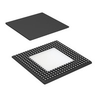
CYV15G0204TRB-BGXC Cypress Semiconductor Corp, CYV15G0204TRB-BGXC Datasheet - Page 17

CYV15G0204TRB-BGXC
Manufacturer Part Number
CYV15G0204TRB-BGXC
Description
IC,TV/VIDEO CIRCUIT,Data Serializer,BICMOS,BGA,256PIN,PLASTIC
Manufacturer
Cypress Semiconductor Corp
Datasheet
1.CYV15G0204TRB-BGXC.pdf
(31 pages)
Specifications of CYV15G0204TRB-BGXC
Function
Serializer/Deserializer
Data Rate
1.485Gbps
Input Type
LVTTL
Output Type
PECL
Number Of Inputs
4
Number Of Outputs
4
Voltage - Supply
3.15 V ~ 3.45 V
Operating Temperature
0°C ~ 70°C
Mounting Type
Surface Mount
Package / Case
256-LBGA Exposed Pad, 32-HLBGA
Lead Free Status / RoHS Status
Lead free / RoHS Compliant
Available stocks
Company
Part Number
Manufacturer
Quantity
Price
Company:
Part Number:
CYV15G0204TRB-BGXC
Manufacturer:
Cypress Semiconductor Corp
Quantity:
135
Company:
Part Number:
CYV15G0204TRB-BGXC
Manufacturer:
Cypress
Quantity:
80
Company:
Part Number:
CYV15G0204TRB-BGXC
Manufacturer:
CYPRESS
Quantity:
216
Company:
Part Number:
CYV15G0204TRB-BGXC
Manufacturer:
Cypress Semiconductor Corp
Quantity:
10 000
Document Number : 38-02101 Rev. *D
Table 4. Device Configuration and Control Latch Descriptions (continued)
RXRATEC
RXRATED
SDASEL1C[1:0]
SDASEL1D[1:0]
SDASEL2C[1:0]
SDASEL2D[1:0]
TRGRATEC
TRGRATED
RXPLLPDC
RXPLLPDD
RXBISTC[1:0]
RXBISTD[1:0]
ROE2C
ROE2D
ROE1C
ROE1D
Name
Receive Clock Rate Select. The initialization value of the RXRATEx latch = 1. RXRATEx is used to select
the rate of the RXCLKx± clock output.
When RXRATEx = 1, the RXCLKx± clock outputs are complementary clocks that follow the recovered clock
operating at half the character rate. Data for the associated receive channels should be latched alternately
on the rising edge of RXCLKx+ and RXCLKx–.
When RXRATEx = 0, the RXCLKx± clock outputs are complementary clocks that follow the recovered clock
operating at the character rate. Data for the associated receive channels should be latched on the rising edge
of RXCLKx+ or falling edge of RXCLKx–.
Primary Serial Data Input Signal Detector Amplitude Select. The initialization value of the SDASEL1x[1:0]
latch = 10. SDASEL1x[1:0] selects the trip point for the detection of a valid signal for the INx1± Primary
Differential Serial Data Inputs.
When SDASEL1x[1:0] = 00, the Analog Signal Detector is disabled.
When SDASEL1x[1:0] = 01, the typical p-p differential voltage threshold level is 140 mV.
When SDASEL1x[1:0] = 10, the typical p-p differential voltage threshold level is 280 mV.
When SDASEL1x[1:0] = 11, the typical p-p differential voltage threshold level is 420 mV.
Secondary Serial Data Input Signal Detector Amplitude Select. The initialization value of the
SDASEL2x[1:0] latch = 10. SDASEL2x[1:0] selects the trip point for the detection of a valid signal for the INx2±
Secondary Differential Serial Data Inputs.
When SDASEL2x[1:0] = 00, the Analog Signal Detector is disabled
When SDASEL2x[1:0] = 01, the typical p-p differential voltage threshold level is 140 mV.
When SDASEL2x[1:0] = 10, the typical p-p differential voltage threshold level is 280 mV.
When SDASEL2x[1:0] = 11, the typical p-p differential voltage threshold level is 420 mV.
the clock multiplier for the training clock input to the associated CDR PLL. When TRGRATEx = 0, the
TRGCLKx± input is not multiplied before it is passed to the CDR PLL. When TRGRATEx = 1, the TRGCLKx±
input is multiplied by 2 before it is passed to the CDR PLL. TRGRATEx = 1 and SPDSELx = LOW is an invalid
state and this combination is reserved.
Receive Channel Enable. The initialization value of the RXPLLPDx latch = 0. RXPLLPDx selects if the
associated receive channel is enabled or powered-down. When RXPLLPDx = 0, the associated receive PLL
and analog circuitry are powered-down. When RXPLLPDx = 1, the associated receive PLL and analog circuitry
are enabled.
Receive Bist Disable / SMPTE Receive Enable. The initialization value of the RXBISTx[1:0] latch = 11. For
SMPTE data reception, RXBISTx[1:0] should not remain in this initialization state (11). RXBISTx[1:0] selects
if receive BIST is disabled or enabled and sets the associated channel for SMPTE data reception. When
RXBISTx[1:0] = 01, the receiver BIST function is disabled and the associated channel is set to receive SMPTE
data. When RXBISTx[1:0] = 10, the receive BIST function is enabled and the associated channel is set to
receive BIST data. RXBISTx[1:0] = 00 and RXBISTx[1:0] = 11 are invalid states.
Reclocker Secondary Differential Serial Data Output Driver Enable. The initialization value of the ROE2x
latch = 0. ROE2x selects if the ROUTx2± secondary differential output drivers are enabled or disabled. When
ROE2x = 1, the associated serial data output driver is enabled allowing data to be transmitted from the transmit
shifter. When ROE2x = 0, the associated serial data output driver is disabled. When a driver is disabled via
the configuration interface, it is internally powered down to reduce device power. If both serial drivers for a
channel are in this disabled state, the associated internal logic for that channel is also powered down. A device
reset (RESET sampled LOW) disables all output drivers.
Reclocker Primary Differential Serial Data Output Driver Enable. The initialization value of the ROE1x
latch = 0. ROE1x selects if the ROUTx1± primary differential output drivers are enabled or disabled. When
ROE1x = 1, the associated serial data output driver is enabled allowing data to be transmitted from the transmit
shifter. When ROE1x = 0, the associated serial data output driver is disabled. When a driver is disabled via
the configuration interface, it is internally powered down to reduce device power. If both serial drivers for a
channel are in this disabled state, the associated internal logic for that channel is also powered down. A device
reset (RESET sampled LOW) disables all output drivers.
Training Clock Rate Select. The initialization value of the TRGRATEx latch = 0. TRGRATEx is used to select
Signal Description
CYV15G0204TRB
Page 17 of 31
[+] Feedback


