CYV15G0204TRB-BGXC Cypress Semiconductor Corp, CYV15G0204TRB-BGXC Datasheet - Page 12
CYV15G0204TRB-BGXC
Manufacturer Part Number
CYV15G0204TRB-BGXC
Description
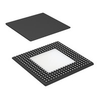
IC,TV/VIDEO CIRCUIT,Data Serializer,BICMOS,BGA,256PIN,PLASTIC
Manufacturer
Cypress Semiconductor Corp
Datasheet
1.CYV15G0204TRB-BGXC.pdf
(31 pages)
Specifications of CYV15G0204TRB-BGXC
Function
Serializer/Deserializer
Data Rate
1.485Gbps
Input Type
LVTTL
Output Type
PECL
Number Of Inputs
4
Number Of Outputs
4
Voltage - Supply
3.15 V ~ 3.45 V
Operating Temperature
0°C ~ 70°C
Mounting Type
Surface Mount
Package / Case
256-LBGA Exposed Pad, 32-HLBGA
Lead Free Status / RoHS Status
Lead free / RoHS Compliant
Available stocks
Company
Part Number
Manufacturer
Quantity
Price
Company:

Part Number:
CYV15G0204TRB-BGXC
Manufacturer:
Cypress Semiconductor Corp
Quantity:
135
Company:
Part Number:
CYV15G0204TRB-BGXC
Manufacturer:
Cypress
Quantity:
80
Company:
Part Number:
CYV15G0204TRB-BGXC
Manufacturer:
CYPRESS
Quantity:
216
Company:
Part Number:
CYV15G0204TRB-BGXC
Manufacturer:
Cypress Semiconductor Corp
Quantity:
10 000


Document Number : 38-02101 Rev. *D
Pin Definitions
CYV15G0204TRB HOTLink II Dual Serializer and Dual Reclocking Deserializer
CYV15G0204TRB HOTLink II Operation
The CYV15G0204TRB is a highly configurable, independent
clocking, device designed to support reliable transfer of large
quantities of digital video data, using high-speed serial links
from multiple sources to multiple destinations.
CYV15G0204TRB Transmit Data Path
Input Register
The parallel input bus TXDx[9:0] can be clocked in using
TXCLKx (TXCKSELx = 0) or REFCLKx (TXCKSELx = 1).
Phase-Align Buffer
Data from each Input Register is passed to the associated
Phase-Align Buffer, when the TXDx[9:0] input registers are
clocked using TXCLKx (TXCKSELx = 0 and TXRATEx = 0).
When the TXDx[9:0] input registers are clocked using
REFCLKx± (TXCKSELx = 1) and REFCLKx± is a full-rate
clock, the associated Phase Alignment Buffer in the transmit
path is bypassed. These buffers are used to absorb clock
phase differences between the TXCLKx input clock and the
internal character clock for that channel.
Once initialized, TXCLKx is allowed to drift in phase as much
as ±180 degrees. If the input phase of TXCLKx drifts beyond
the handling capacity of the Phase Align Buffer, TXERRx is
asserted to indicate the loss of data, and remains asserted
until the Phase Align Buffer is initialized. The phase of the
TXCLKx relative to its associated internal character rate clock
is initialized when the configuration latch PABRSTx is written
as 0. When the associated TXERRx is deasserted, the Phase
Align Buffer is initialized and input characters are correctly
captured.
If the phase offset, between the initialized location of the input
clock and REFCLKx, exceeds the skew handling capabilities
INC2±
IND2±
TMS
TCLK
TDO
TDI
TRST
V
GND
Name
JTAG Interface
Power
CC
(continued)
Differential Input
LVTTL Input,
internal pull-up
LVTTL Input,
internal pull-down
3-State LVTTL
Output
LVTTL Input,
internal pull-up
LVTTL Input,
internal pull-up
I/O Characteristics Signal Description
Secondary Differential Serial Data Input. The INx2± input accepts the serial data
stream for deserialization. The INx2± serial stream is passed to the receiver CDR
circuit to extract the data content when INSELx = LOW.
Test Mode Select. Used to control access to the JTAG Test Modes. If maintained
high for 5 TCLK cycles, the JTAG test controller is reset.
JTAG Test Clock.
Test Data Out. JTAG data output buffer. High-Z while JTAG test mode is not
selected.
Test Data In. JTAG data input port.
JTAG reset signal. When asserted (LOW), this input asynchronously resets the
JTAG test access port controller.
+3.3V Power.
Signal and Power Ground for all internal circuits.
of the Phase-Align Buffer, an error is reported on that
channel’s TXERRx output. This output indicates an error
continuously until the Phase-Align Buffer for that channel is
reset. While the error remains active, the transmitter for that
channel outputs a continuous “1001111000” character to
indicate to the remote receiver that an error condition is
present in the link.
Transmit BIST
Each transmit channel contains an internal pattern generator
that can be used to validate both the link and device operation.
These generators are enabled by the associated TXBISTx
latch via the device configuration interface. When enabled, a
register in the associated transmit channel becomes a
signature pattern generator by logically converting to a Linear
Feedback Shift Register (LFSR). This LFSR generates a
511-character sequence. This provides a predictable yet
pseudo-random sequence that can be matched to an identical
LFSR in the attached Receiver(s).
A device reset (RESET sampled LOW) presets the BIST
Enable Latches to disable BIST on both channels.
All data present at the associated TXDx[9:0] inputs are ignored
when BIST is active on that channel.
Transmit PLL Clock Multiplier
Each Transmit PLL Clock Multiplier accepts a character-rate
or half-character-rate external clock at the associated
REFCLKx± input, and that clock is multiplied by 10 or 20 (as
selected by TXRATEx) to generate a bit-rate clock for use by
the transmit shifter. It also provides a character-rate clock used
by the transmit paths, and outputs this character rate clock as
TXCLKOx.
Each clock multiplier PLL can accept a REFCLKx± input
between 19.5 MHz and 150 MHz, however, this clock range is
limited by the operating mode of the CYV15G0204TRB clock
CYV15G0204TRB
Page 12 of 31
[+] Feedback
Related parts for CYV15G0204TRB-BGXC
Image
Part Number
Description
Manufacturer
Datasheet
Request
R

Part Number:
Description:
Manufacturer:
Cypress Semiconductor Corp
Datasheet:
Part Number:
Description:
Manufacturer:
Cypress Semiconductor Corp
Datasheet:
Part Number:
Description:
Manufacturer:
Cypress Semiconductor Corp
Datasheet:
Part Number:
Description:
Manufacturer:
Cypress Semiconductor Corp
Datasheet:
Part Number:
Description:
Manufacturer:
Cypress Semiconductor Corp
Datasheet: