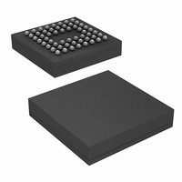
CY7C68053-56BAXIT Cypress Semiconductor Corp, CY7C68053-56BAXIT Datasheet - Page 13

CY7C68053-56BAXIT
Manufacturer Part Number
CY7C68053-56BAXIT
Description
CY7C68053-56BAXIT
Manufacturer
Cypress Semiconductor Corp
Series
MoBL-USB™r
Datasheet
1.CY7C68053-56BAXI.pdf
(42 pages)
Specifications of CY7C68053-56BAXIT
Applications
USB Microcontroller
Core Processor
8051
Program Memory Type
ROMless
Controller Series
CY7C680xx
Ram Size
16K x 8
Interface
I²C, USB
Number Of I /o
56
Voltage - Supply
1.71 V ~ 1.89 V
Operating Temperature
-40°C ~ 85°C
Mounting Type
Surface Mount
Package / Case
56-VFBGA
Processor Series
CY7C68xx
Core
8051
Data Bus Width
8 bit
Data Ram Size
16 KB
Interface Type
I2C
Maximum Clock Frequency
48 MHz
Number Of Programmable I/os
24
Maximum Operating Temperature
+ 85 C
Mounting Style
SMD/SMT
Minimum Operating Temperature
- 40 C
Lead Free Status / RoHS Status
Lead free / RoHS Compliant
For Use With
CY3687 - KIT DEV MOBL-USB FX2LP18
Lead Free Status / Rohs Status
Details
Available stocks
Company
Part Number
Manufacturer
Quantity
Price
Company:
Part Number:
CY7C68053-56BAXIT
Manufacturer:
Cypress Semiconductor Corp
Quantity:
10 000
4.1 CY7C68053 Pin Descriptions
Table 7. FX2LP18 Pin Descriptions
Document # 001-06120 Rev *J
Note
56 VFBGA
9. Do not leave unused inputs floating. Tie either HIGH or LOW as appropriate. Only pull outputs up or down to ensure signals at power up and in standby. Do not drive
Port A
any pins while the device is powered down.
8G
6G
2D
1D
2F
1F
1E
2E
8B
1C
2C
2B
8F
7F
AV
AV
AGND
AGND
DMINUS
DPLUS
RESET#
XTALIN
XTALOUT
CLKOUT
PA0 or
INT0#
PA1 or
INT1#
PA2 or
SLOE
PA3 or
WU2
CC
CC
Name
Ground
Ground
Output
Power
Power
Type
I/O/Z
I/O/Z
Input
Input
I/O/Z
I/O/Z
I/O/Z
I/O/Z
O/Z
[9]
12 MHz
Default
(PA0)
(PA1)
(PA2)
(PA3)
N/A
N/A
N/A
N/A
N/A
N/A
N/A
Z
Z
I
I
I
I
Analog VCC. Connect this pin to 3.3 V power source. This signal provides
power to the analog section of the chip.
Provide an appropriate bulk/bypass capacitance for this supply rail.
Analog VCC. Connect this pin to 3.3 V power source. This signal provides
power to the analog section of the chip.
Analog Ground. Connect this pin to ground with as short a path as possible.
Analog Ground. Connect to this pin ground with as short a path as possible.
USB D– Signal. Connect this pin to the USB D– signal.
USB D+ Signal. Connect this pin to the USB D+ signal.
Active LOW Reset. This pin resets the entire chip. See
page 6
Crystal Input. Connect this signal to a 24 MHz parallel resonant, fundamental
mode crystal and load capacitor to GND.
It is also correct to drive XTALIN with an external 24 MHz square wave derived
from another clock source.
Crystal Output. Connect this signal to a 24 MHz parallel resonant, funda-
mental mode crystal and load capacitor to GND.
If an external clock is used to drive XTALIN, leave this pin open.
CLKOUT. 12, 24, or 48 MHz clock, phase locked to the 24 MHz input clock.
The 8051 defaults to 12 MHz operation. The 8051 may tri-state this output by
setting CPUCS.1 = 1.
Multiplexed pin whose function is selected by PORTACFG.0
PA0 is a bidirectional I/O port pin.
INT0# is the active LOW 8051 INT0 interrupt input signal, which is either edge
triggered (IT0 = 1) or level triggered (IT0 = 0).
Multiplexed pin whose function is selected by PORTACFG.1
PA1 is a bidirectional I/O port pin.
INT1# is the active LOW 8051 INT1 interrupt input signal, which is either edge
triggered (IT1 = 1) or level triggered (IT1 = 0).
Multiplexed pin whose function is selected by two bits: IFCONFIG[1:0].
PA2 is a bidirectional I/O port pin.
SLOE is an input-only output enable with programmable polarity (FIFOPIN-
POLAR.4) for the slave FIFO’s connected to FD[7:0] or FD[15:0].
Multiplexed pin whose function is selected by: WAKEUP.7 and OEA.3
PA3 is a bidirectional I/O port pin.
WU2 is an alternate source for USB Wakeup, enabled by WU2EN bit
(WAKEUP.1) and polarity set by WU2POL (WAKEUP.4). If the 8051 is in
suspend and WU2EN = 1, a transition on this pin starts up the oscillator and
interrupts the 8051 to allow it to exit the suspend mode. Asserting this pin
inhibits the chip from suspending, if WU2EN = 1.
for details.
Description
Reset and Wakeup on
CY7C68053
Page 13 of 42
[+] Feedback


