CY7C68053-56BAXI Cypress Semiconductor Corp, CY7C68053-56BAXI Datasheet - Page 35
CY7C68053-56BAXI
Manufacturer Part Number
CY7C68053-56BAXI
Description
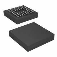
IC,MICROCONTROLLER,8-BIT,8051 CPU,BGA,56PIN,PLASTIC
Manufacturer
Cypress Semiconductor Corp
Series
MoBL-USB™r
Datasheet
1.CY7C68053-56BAXI.pdf
(42 pages)
Specifications of CY7C68053-56BAXI
Applications
USB Microcontroller
Core Processor
8051
Program Memory Type
ROMless
Controller Series
CY7C680xx
Ram Size
16K x 8
Interface
I²C, USB
Number Of I /o
56
Voltage - Supply
1.71 V ~ 1.89 V
Operating Temperature
-40°C ~ 85°C
Mounting Type
Surface Mount
Package / Case
56-VFBGA
Processor Series
CY7C68xx
Core
8051
Data Bus Width
8 bit
Data Ram Size
16 KB
Interface Type
I2C
Maximum Clock Frequency
48 MHz
Number Of Programmable I/os
24
Maximum Operating Temperature
+ 85 C
Mounting Style
SMD/SMT
Minimum Operating Temperature
- 40 C
Lead Free Status / RoHS Status
Lead free / RoHS Compliant
For Use With
CY3687 - KIT DEV MOBL-USB FX2LP18
Lead Free Status / Rohs Status
Details
Available stocks
Company
Part Number
Manufacturer
Quantity
Price
Company:

Part Number:
CY7C68053-56BAXI
Manufacturer:
Cypress Semiconductor Corp
Quantity:
10 000
Company:
Part Number:
CY7C68053-56BAXIT
Manufacturer:
Cypress Semiconductor Corp
Quantity:
10 000


9.13.3 Sequence Diagram of a Single and Burst Asynchronous Read
Figure 23
signals during an asynchronous FIFO read. It shows a single
read followed by a burst read.
■
■
■
Document # 001-06120 Rev *J
At t = 0, the FIFO address is stable and the SLCS signal is
asserted.
At t = 1, SLOE is asserted. This results in the data bus being
driven. The data that is driven on to the bus is previous data;
it is data that was in the FIFO from a prior read cycle.
At t = 2, SLRD is asserted. The SLRD must meet the minimum
active pulse of t
t
SLRD is asserted (that is, the SLCS and SLRD signals must
both be asserted to start a valid read condition).
RDpwh
FIFOADR
FLAGS
FIFO POINTER
FIFO DATA BUS Not Driven
DATA
SLRD
SLCS
SLOE
. If SLCS is used then, SLCS must be asserted before
illustrates the timing relationship of the SLAVE FIFO
RDpwl
t=0
t=1
N
Figure 23. Slave FIFO Asynchronous Read Sequence and Timing Diagram
Driven
Data (X)
and minimum inactive pulse width of
t
SFA
t
OEon
Figure 24. Slave FIFO Asynchronous Read Sequence of Events Diagram
SLOE
t=2
t
RDpwl
Driven: X
t
XFD
t=3
N
N
t=4
t
RDpwh
t
FAH
SLRD
t
OEoff
t
XFLG
N
N
SLRD
T=0
N+1
T=1
N
SLOE
t
t
SFA
OEon
N
T=2
Not Driven
t
N+1
RDpwl
t
XFD
T=3
SLOE
■
The same sequence of events is also shown for a burst read
marked with T = 0 through 5.
Note In burst read mode, during SLOE assertion, the data bus
is in a driven state and outputs the previous data. Once SLRD is
asserted, the data from the FIFO is driven on the data bus (SLOE
must also be asserted) and then the FIFO pointer is
incremented.
The data that is driven, after asserting SLRD, is the updated
data from the FIFO. This data is valid after a propagation delay
of t
is the first valid data read from the FIFO. For data to appear on
the data bus during the read cycle (for example, SLRD is
asserted), SLOE MUST be in an asserted state. SLRD and
SLOE can also be tied together.
t
N+1
RDpwh
XFD
N+1
N
T=4
SLRD
from the activating edge of SLRD. In
t
RDpwl
t
XFD
N+1
T=5
N+1
SLRD
t
N+2
RDpwh
N+2
T=6
N+1
SLRD
t
RDpwl
t
XFD
N+3
N+2
N+2
T=7
t
t
RDpwh
FAH
[16]
SLRD
t
OEoff
t
XFLG
N+3
N+2
CY7C68053
Figure
SLOE
Page 35 of 42
Not Driven
23, data N
N+3
[+] Feedback
Related parts for CY7C68053-56BAXI
Image
Part Number
Description
Manufacturer
Datasheet
Request
R

Part Number:
Description:
CY7C68053-56BAXIT
Manufacturer:
Cypress Semiconductor Corp
Datasheet:

Part Number:
Description:
Manufacturer:
Cypress Semiconductor Corp
Datasheet:
Part Number:
Description:
Manufacturer:
Cypress Semiconductor Corp
Datasheet:
Part Number:
Description:
Manufacturer:
Cypress Semiconductor Corp
Datasheet:
Part Number:
Description:
Manufacturer:
Cypress Semiconductor Corp
Datasheet:
Part Number:
Description:
Manufacturer:
Cypress Semiconductor Corp
Datasheet: