CY7C68053-56BAXI Cypress Semiconductor Corp, CY7C68053-56BAXI Datasheet - Page 14
CY7C68053-56BAXI
Manufacturer Part Number
CY7C68053-56BAXI
Description
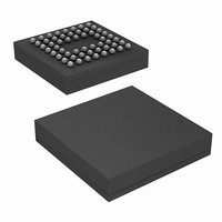
IC,MICROCONTROLLER,8-BIT,8051 CPU,BGA,56PIN,PLASTIC
Manufacturer
Cypress Semiconductor Corp
Series
MoBL-USB™r
Datasheet
1.CY7C68053-56BAXI.pdf
(42 pages)
Specifications of CY7C68053-56BAXI
Applications
USB Microcontroller
Core Processor
8051
Program Memory Type
ROMless
Controller Series
CY7C680xx
Ram Size
16K x 8
Interface
I²C, USB
Number Of I /o
56
Voltage - Supply
1.71 V ~ 1.89 V
Operating Temperature
-40°C ~ 85°C
Mounting Type
Surface Mount
Package / Case
56-VFBGA
Processor Series
CY7C68xx
Core
8051
Data Bus Width
8 bit
Data Ram Size
16 KB
Interface Type
I2C
Maximum Clock Frequency
48 MHz
Number Of Programmable I/os
24
Maximum Operating Temperature
+ 85 C
Mounting Style
SMD/SMT
Minimum Operating Temperature
- 40 C
Lead Free Status / RoHS Status
Lead free / RoHS Compliant
For Use With
CY3687 - KIT DEV MOBL-USB FX2LP18
Lead Free Status / Rohs Status
Details
Available stocks
Company
Part Number
Manufacturer
Quantity
Price
Company:

Part Number:
CY7C68053-56BAXI
Manufacturer:
Cypress Semiconductor Corp
Quantity:
10 000
Company:
Part Number:
CY7C68053-56BAXIT
Manufacturer:
Cypress Semiconductor Corp
Quantity:
10 000


Table 7. FX2LP18 Pin Descriptions (continued)
Document # 001-06120 Rev *J
Port B
56 VFBGA
4G
5G
6F
8C
7C
6C
3H
4F
4H
5H
5F
6H
PA4 or
FIFOADR0
PA5 or
FIFOADR1
PA6 or
PKTEND
PA7 or
FLAGD or
SLCS#
PB0 or
FD[0]
PB1 or
FD[1]
PB2 or
FD[2]
PB3 or
FD[3]
PB4 or
FD[4]
PB5 or
FD[5]
PB6 or
FD[6]
PB7 or
FD[7]
Name
Type
I/O/Z
I/O/Z
I/O/Z
I/O/Z
I/O/Z
I/O/Z
I/O/Z
I/O/Z
I/O/Z
I/O/Z
I/O/Z
I/O/Z
Default
(PA4)
(PA5)
(PA6)
(PA7)
(PB0)
(PB1)
(PB2)
(PB3)
(PB4)
(PB5)
(PB6)
(PB7)
I
I
I
I
I
I
I
I
I
I
I
I
[9]
Multiplexed pin whose function is selected by IFCONFIG[1:0].
PA4 is a bidirectional I/O port pin.
FIFOADR0 is an input-only address select for the slave FIFOs connected to
FD[7:0] or FD[15:0].
Multiplexed pin whose function is selected by IFCONFIG[1:0].
PA5 is a bidirectional I/O port pin.
FIFOADR1 is an input-only address select for the slave FIFOs connected to
FD[7:0] or FD[15:0].
Multiplexed pin whose function is selected by the IFCONFIG[1:0] bits.
PA6 is a bidirectional I/O port pin.
PKTEND is an input that commits the FIFO packet data to the endpoint and
whose polarity is programmable using FIFOPINPOLAR.5.
Multiplexed pin whose function is selected by the IFCONFIG[1:0] and
PORTACFG.7 bits.
PA7 is a bidirectional I/O port pin.
FLAGD is a programmable slave FIFO output status flag signal.
SLCS# gates all other slave FIFO enable/strobes
Multiplexed pin whose function is selected by IFCONFIG[1:0].
PB0 is a bidirectional I/O port pin.
FD[0] is the bidirectional FIFO/GPIF data bus.
Multiplexed pin whose function is selected by IFCONFIG[1:0].
PB1 is a bidirectional I/O port pin.
FD[1] is the bidirectional FIFO/GPIF data bus.
Multiplexed pin whose function is selected by IFCONFIG[1:0].
PB2 is a bidirectional I/O port pin.
FD[2] is the bidirectional FIFO/GPIF data bus.
Multiplexed pin whose function is selected by IFCONFIG[1:0].
PB3 is a bidirectional I/O port pin.
FD[3] is the bidirectional FIFO/GPIF data bus.
Multiplexed pin whose function is selected by IFCONFIG[1:0].
PB4 is a bidirectional I/O port pin.
FD[4] is the bidirectional FIFO/GPIF data bus.
Multiplexed pin whose function is selected by IFCONFIG[1:0].
PB5 is a bidirectional I/O port pin.
FD[5] is the bidirectional FIFO/GPIF data bus.
Multiplexed pin whose function is selected by IFCONFIG[1:0].
PB6 is a bidirectional I/O port pin.
FD[6] is the bidirectional FIFO/GPIF data bus.
Multiplexed pin whose function is selected IFCONFIG[1:0].
PB7 is a bidirectional I/O port pin.
FD[7] is the bidirectional FIFO/GPIF data bus.
Description
CY7C68053
Page 14 of 42
[+] Feedback
Related parts for CY7C68053-56BAXI
Image
Part Number
Description
Manufacturer
Datasheet
Request
R

Part Number:
Description:
CY7C68053-56BAXIT
Manufacturer:
Cypress Semiconductor Corp
Datasheet:

Part Number:
Description:
Manufacturer:
Cypress Semiconductor Corp
Datasheet:
Part Number:
Description:
Manufacturer:
Cypress Semiconductor Corp
Datasheet:
Part Number:
Description:
Manufacturer:
Cypress Semiconductor Corp
Datasheet:
Part Number:
Description:
Manufacturer:
Cypress Semiconductor Corp
Datasheet:
Part Number:
Description:
Manufacturer:
Cypress Semiconductor Corp
Datasheet: