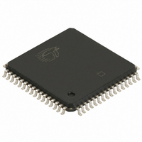
CY7C4265-10AXI Cypress Semiconductor Corp, CY7C4265-10AXI Datasheet - Page 5

CY7C4265-10AXI
Manufacturer Part Number
CY7C4265-10AXI
Description
IC,FIFO,16KX18,SYNCHRONOUS,CMOS,QFP,64PIN,PLASTIC
Manufacturer
Cypress Semiconductor Corp
Series
CY7Cr
Datasheet
1.CY7C4265-15AXC.pdf
(25 pages)
Specifications of CY7C4265-10AXI
Function
Synchronous
Memory Size
288K (16K x 18)
Data Rate
100MHz
Access Time
8ns
Voltage - Supply
3.3V
Operating Temperature
-40°C ~ 85°C
Mounting Type
Surface Mount
Package / Case
64-LQFP
Lead Free Status / RoHS Status
Lead free / RoHS Compliant
Available stocks
Company
Part Number
Manufacturer
Quantity
Price
Company:
Part Number:
CY7C4265-10AXI
Manufacturer:
Cypress Semiconductor Corp
Quantity:
10 000
Maximum Ratings
Exceeding maximum ratings may impair the useful life of the
device. These user guidelines are not tested.
Storage Temperature ................................ –65°C to +150°C
Ambient Temperature with Power Applied. –55°C to +125°C
Supply Voltage to Ground Potential................–0.5V to +7.0V
DC Voltage Applied to Outputs
in High Z State ................................................–0.5V to +7.0V
DC Input Voltage ......................................... −0.5V to V
Electrical Characteristics
Capacitance
Document #: 38-06004 Rev. *G
V
V
V
V
I
I
I
I
I
C
C
Notes
IX
OZL
OZH
CC1
CC2
Parameter
Parameter
2. The Voltage on any input or I/O pin cannot exceed the power pin during power up.
3. T
4. See the last page of this specification for Group A subgroup testing information.
5. The V
6. Input signals switch from 0V to 3V with a rise/fall time of less than 3 ns, clocks and clock enables switch at 20 MHz, while data inputs switch at 10 MHz. Outputs are
7. All inputs = V
8. Tested initially and after any design changes that may affect these parameters.
9. Tested initially and after any process changes that may affect these parameters.
OH
OL
IH
IL
IN
OUT
[5]
[5]
or V
unloaded. I
[6]
[7]
A
is the “Instant On” case temperature.
SS
IH
.
and V
CC
Input Capacitance
Output Capacitance
Output HIGH Voltage
Output LOW Voltage
Input HIGH Voltage
Input LOW Voltage
Input Leakage
Current
Output OFF,
High Z Current
Active Power Supply
Current
Average Standby
Current
CC
1(typical) = (25 mA + (freq – 20 MHz) * (1.0 mA/MHz)).
IL
specifications apply for all inputs except WXI, RXI. The WXI, RXI pin is not a TTL input. It is connected to either RXO, WXO of the previous device
– 0.2V, except RCLK and WCLK (which are switching at frequency = 20 MHz), and FL/RT which is at V
[8, 9]
Description
Description
Over the Operating Range
T
V
V
I
V
I
V
OE > V
V
OH
OL
A
CC
CC
CC
SS
CC
= 25°C, f = 1 MHz,
= 8.0 mA
= –2.0 mA
< V
= Min.,
= Min.,
= Max.
= 5.0V
Test Conditions
Test Conditions
[2]
IH
O
,
< V
CC
CC
Commercial
Industrial
Commercial
Industrial
+0.5V
[4]
–0.5
Output Current into Outputs (LOW)............................. 20 mA
Static Discharge Voltage............................................ >2001V
(per MIL–STD–883, Method 3015)
Latch Up Current ..................................................... >200 mA
Operating Range
Min
–10
–10
2.4
2.0
Commercial
Industrial
7C42X5-10
Range
Max
V
+10
+10
0.4
0.8
45
50
10
15
CC
[4]
–0.5
7C4265A-15
Min
–10
–10
Max
2.4
2.0
5
7
7C42X5,
Max
V
+10
+10
–40°C to +85°C
0.4
0.8
Temperature
45
50
10
15
CC
0°C to +70°C
Ambient
–0.5
SS
Min
–10
–10
2.4
2.0
7C42X5-25
. All outputs are unloaded.
[3]
Max
V
+10
+10
0.4
0.8
45
50
10
15
CC
–0.5
Min
–10
–10
2.4
2.0
7C42X5-35
CY7C4265
Unit
5V ± 10%
5V ± 10%
pF
pF
V
Page 5 of 25
Max
V
+10
+10
CC
0.4
0.8
45
50
10
15
CC
Unit
mA
mA
mA
mA
μA
μA
V
V
V
V
[+] Feedback


