CY7C1471V33-133AXC Cypress Semiconductor Corp, CY7C1471V33-133AXC Datasheet - Page 23
CY7C1471V33-133AXC
Manufacturer Part Number
CY7C1471V33-133AXC
Description
SRAM (Static RAM)
Manufacturer
Cypress Semiconductor Corp
Datasheet
1.CY7C1471V33-133AXC.pdf
(36 pages)
Specifications of CY7C1471V33-133AXC
Format - Memory
RAM
Memory Type
SRAM - Synchronous
Memory Size
72M (2M x 36)
Speed
133MHz
Interface
Parallel
Voltage - Supply
3.135 V ~ 3.6 V
Operating Temperature
0°C ~ 70°C
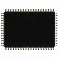
Package / Case
100-LQFP
Density
72Mb
Access Time (max)
6.5ns
Sync/async
Synchronous
Architecture
SDR
Clock Freq (max)
133MHz
Operating Supply Voltage (typ)
3.3V
Address Bus
21b
Package Type
TQFP
Operating Temp Range
0C to 70C
Number Of Ports
4
Supply Current
305mA
Operating Supply Voltage (min)
3.135V
Operating Supply Voltage (max)
3.6V
Operating Temperature Classification
Commercial
Mounting
Surface Mount
Pin Count
100
Word Size
36b
Number Of Words
2M
Lead Free Status / RoHS Status
Lead free / RoHS Compliant
Lead Free Status / RoHS Status
Lead free / RoHS Compliant
Other names
428-2167
CY7C1471V33-133AXC
CY7C1471V33-133AXC
Available stocks
Company
Part Number
Manufacturer
Quantity
Price
Company:

Part Number:
CY7C1471V33-133AXC
Manufacturer:
Cypress Semiconductor Corp
Quantity:
135
Company:
Part Number:
CY7C1471V33-133AXC
Manufacturer:
TOSHIBA
Quantity:
2 100
Company:
Part Number:
CY7C1471V33-133AXC
Manufacturer:
Cypress Semiconductor Corp
Quantity:
10 000
Part Number:
CY7C1471V33-133AXC
Manufacturer:
CYPRESS/赛普拉斯
Quantity:
20 000
Company:
Part Number:
CY7C1471V33-133AXCT
Manufacturer:
Cypress Semiconductor Corp
Quantity:
10 000


Maximum Ratings
Exceeding maximum ratings may impair the useful life of the
device. These user guidelines are not tested.
Storage temperature ................................ –65 C to +150 C
Ambient temperature with
power applied ........................................... –55 C to +125 C
Supply voltage on V
Supply voltage on V
DC voltage applied to outputs
in tri-state...........................................–0.5 V to V
Electrical Characteristics
Over the Operating Range
Notes
Document Number: 38-05288 Rev. *L
V
V
V
V
V
V
I
I
I
I
I
I
I
16. Overshoot: V
17. T
Parameter
X
OZ
DD
SB1
SB2
SB3
SB4
DD
DDQ
OH
OL
IH
IL
Power-up
: assumes a linear ramp from 0 V to V
Power supply voltage
IO supply voltage
Output HIGH voltage
Output LOW voltage
Input HIGH voltage
Input LOW voltage
Input leakage current
except ZZ and MODE
Input current of MODE
Input current of ZZ
Output leakage current GND V
V
current
Automatic CE
power-down
current—TTL inputs
Automatic CE
power-down
current—CMOS inputs
Automatic CE
power-down
current—CMOS inputs
Automatic CE
power-down
current—TTL inputs
IH
DD
(AC) < V
operating supply
Description
DD
DDQ
DD
relative to GND ........–0.5 V to +4.6 V
+ 1.5 V (pulse width less than t
relative to GND....... –0.5 V to +V
[16, 17]
[16]
[16]
For 3.3 V IO
For 2.5 V IO
For 3.3 V IO, I
For 2.5 V IO, I
For 3.3 V IO, I
For 2.5 V IO, I
For 3.3 V IO
For 2.5 V IO
For 3.3 V IO
For 2.5 V IO
GND V
Input = V
Input = V
Input = V
Input = V
V
f = f
V
V
f = f
V
V
f = 0, inputs static
V
V
f = f
V
V
f = 0, inputs static
DD
DD
DD
IN
DD
IN
DD
IN
DD
IN
(min) within 200 ms. During this time V
MAX
V
MAX
0.3 V or V
0.3 V or V
MAX
V
= Max, I
= Max, device deselected,
= Max, device deselected,
= Max, device deselected, or
= Max, device deselected,
IH
DD
, inputs switching
, inputs switching
= 1/t
I
SS
DD
SS
DD
I
DDQ
or V
CYC
V
V
– 0.3 V or V
OUT
/2). Undershoot: V
CYC
DDQ
DD,
IN
OH
OH
OL
OL
+ 0.5 V
IN
IN
V
= 0 mA,
= 8.0 mA
= 1.0 mA
output disabled
= –4.0 mA
= –1.0 mA
> V
> V
DD
IL
Test Conditions
DDQ
DD
IN
– 0.3 V,
0.3 V,
– 0.3 V
IL
(AC) > –2 V (pulse width less than t
DC input voltage .................................. –0.5 V to V
Current into outputs (LOW) ......................................... 20 mA
Static discharge voltage.......................................... > 2001 V
(MIL-STD-883, method 3015)
Latch-up current .................................................... > 200 mA
Operating Range
Commercial
Industrial
Range
IH
All speeds
All Speeds
7.5 ns cycle, 133 MHz
10 ns cycle, 117 MHz
7.5 ns cycle, 133 MHz
10 ns cycle, 117 MHz
7.5 ns cycle, 133 MHz
10 ns cycle, 117 MHz
< V
DD
and V
–40 C to +85 C
0 C to +70 C
Temperature
DDQ
Ambient
< V
DD
.
CYC
/2).
3.135
3.135
2.375
–0.3
–0.3
Min
–30
2.4
2.0
2.0
1.7
–5
–5
–5
–
–
–
–
–
–
–
–
–
–
–
–
3.3 V– 5% /
+ 10%
V
CY7C1471V33
CY7C1473V33
CY7C1475V33
DD
V
V
DD
DD
2.625
Max
V
305
275
200
200
120
200
200
165
3.6
0.4
0.4
0.8
0.7
30
–
–
+ 0.3V
+ 0.3V
5
–
5
–
5
DD
Page 23 of 36
DD
2.5 V – 5%
to V
V
+ 0.5 V
Unit
mA
mA
mA
mA
mA
mA
mA
mA
A
A
A
A
A
A
DDQ
V
V
V
V
V
V
V
V
V
V
V
DD
[+] Feedback
Related parts for CY7C1471V33-133AXC
Image
Part Number
Description
Manufacturer
Datasheet
Request
R

Part Number:
Description:
IC SRAM 72MBIT 117MHZ 100LQFP
Manufacturer:
Cypress Semiconductor Corp
Datasheet:
Part Number:
Description:
IC SRAM 72MBIT 133MHZ 100LQFP
Manufacturer:
Cypress Semiconductor Corp
Datasheet:
Part Number:
Description:
Manufacturer:
Cypress Semiconductor Corp
Datasheet:
Part Number:
Description:
Manufacturer:
Cypress Semiconductor Corp
Datasheet:
Part Number:
Description:
Manufacturer:
Cypress Semiconductor Corp
Datasheet:
Part Number:
Description:
Manufacturer:
Cypress Semiconductor Corp
Datasheet:
Part Number:
Description:
Manufacturer:
Cypress Semiconductor Corp
Datasheet: