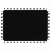
CY7C1471V33-133AXC Cypress Semiconductor Corp, CY7C1471V33-133AXC Datasheet - Page 13

CY7C1471V33-133AXC
Manufacturer Part Number
CY7C1471V33-133AXC
Description
SRAM (Static RAM)
Manufacturer
Cypress Semiconductor Corp
Datasheet
1.CY7C1471V33-133AXC.pdf
(36 pages)
Specifications of CY7C1471V33-133AXC
Format - Memory
RAM
Memory Type
SRAM - Synchronous
Memory Size
72M (2M x 36)
Speed
133MHz
Interface
Parallel
Voltage - Supply
3.135 V ~ 3.6 V
Operating Temperature
0°C ~ 70°C
Package / Case
100-LQFP
Density
72Mb
Access Time (max)
6.5ns
Sync/async
Synchronous
Architecture
SDR
Clock Freq (max)
133MHz
Operating Supply Voltage (typ)
3.3V
Address Bus
21b
Package Type
TQFP
Operating Temp Range
0C to 70C
Number Of Ports
4
Supply Current
305mA
Operating Supply Voltage (min)
3.135V
Operating Supply Voltage (max)
3.6V
Operating Temperature Classification
Commercial
Mounting
Surface Mount
Pin Count
100
Word Size
36b
Number Of Words
2M
Lead Free Status / RoHS Status
Lead free / RoHS Compliant
Lead Free Status / RoHS Status
Lead free / RoHS Compliant
Other names
428-2167
CY7C1471V33-133AXC
CY7C1471V33-133AXC
Available stocks
Company
Part Number
Manufacturer
Quantity
Price
Company:
Part Number:
CY7C1471V33-133AXC
Manufacturer:
Cypress Semiconductor Corp
Quantity:
135
Company:
Part Number:
CY7C1471V33-133AXC
Manufacturer:
TOSHIBA
Quantity:
2 100
Company:
Part Number:
CY7C1471V33-133AXC
Manufacturer:
Cypress Semiconductor Corp
Quantity:
10 000
Part Number:
CY7C1471V33-133AXC
Manufacturer:
CYPRESS/赛普拉斯
Quantity:
20 000
Company:
Part Number:
CY7C1471V33-133AXCT
Manufacturer:
Cypress Semiconductor Corp
Quantity:
10 000
Truth Table
The truth table for CY7C1471V33, CY7C1473V33, CY7C1475V33 follows.
Notes
Document Number: 38-05288 Rev. *L
Deselect cycle
Deselect cycle
Deselect cycle
Continue deselect cycle
Read cycle
(begin burst)
Read cycle
(continue burst)
NOP/dummy read
(begin burst)
Dummy read
(continue burst)
Write cycle
(begin burst)
Write cycle
(continue burst)
NOP/write abort
(begin burst)
Write abort
(continue burst)
Ignore clock edge (stall)
Sleep mode
2. X = “Don't Care.” H = Logic HIGH, L = Logic LOW. BW
3. Write is defined by BW
4. When a Write cycle is detected, all IOs are tri-stated, even during byte writes.
5. The DQs and DQP
6. CEN = H, inserts wait states.
7. Device powers up deselected with the IOs in a tri-state condition, regardless of OE.
8. OE is asynchronous and is not sampled with the clock rise. It is masked internally during write cycles. During a read cycle DQs and DQP
selects are asserted, see
is inactive or when the device is deselected, and DQs and DQP
Operation
X
pins are controlled by the current cycle and the OE signal. OE is asynchronous and is not sampled with the clock.
X
, and WE. See
“Truth Table for Read/Write” on page 14
Address
External
External
External
Current
Used
None
None
None
None
None
None
Next
Next
Next
Next
“Truth Table for Read/Write” on page
CE
H
X
X
X
X
X
X
X
X
X
L
L
L
L
1
X
= L signifies at least one byte write select is active, BW
CE
H
H
H
H
X
X
X
X
X
X
X
X
X
L
2
X
CE
= data when OE is active.
X
H
X
X
X
X
X
X
X
X
for details.
L
L
L
L
3
ZZ
H
L
L
L
L
L
L
L
L
L
L
L
L
L
14.
ADV/LD
H
H
H
H
H
L
L
L
L
L
L
L
X
X
[2, 3, 4, 5, 6, 7, 8]
WE
X
X
X
X
H
X
H
X
X
X
X
X
L
L
BW
X
X
X
X
X
X
X
X
H
H
X
X
L
L
X
X
= valid signifies that the desired byte write
OE
H
H
X
X
X
X
X
X
X
X
X
L
L
X
CEN CLK
H
L
L
L
L
L
L
L
L
L
L
L
L
X
L->H
L->H
L->H
L->H
L->H Data out (Q)
L->H Data out (Q)
L->H
L->H
L->H
L->H
L->H
L->H
L->H
CY7C1471V33
CY7C1473V33
CY7C1475V33
X
X
= tri-state when OE
Data in (D)
Data in (D)
Tri-state
Tri-state
Tri-state
Tri-state
Tri-state
Tri-state
Tri-state
Tri-state
Tri-state
Page 13 of 36
DQ
-
[+] Feedback


