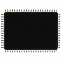
CY7C1471V33-133AXC Cypress Semiconductor Corp, CY7C1471V33-133AXC Datasheet - Page 18

CY7C1471V33-133AXC
Manufacturer Part Number
CY7C1471V33-133AXC
Description
SRAM (Static RAM)
Manufacturer
Cypress Semiconductor Corp
Datasheet
1.CY7C1471V33-133AXC.pdf
(36 pages)
Specifications of CY7C1471V33-133AXC
Format - Memory
RAM
Memory Type
SRAM - Synchronous
Memory Size
72M (2M x 36)
Speed
133MHz
Interface
Parallel
Voltage - Supply
3.135 V ~ 3.6 V
Operating Temperature
0°C ~ 70°C
Package / Case
100-LQFP
Density
72Mb
Access Time (max)
6.5ns
Sync/async
Synchronous
Architecture
SDR
Clock Freq (max)
133MHz
Operating Supply Voltage (typ)
3.3V
Address Bus
21b
Package Type
TQFP
Operating Temp Range
0C to 70C
Number Of Ports
4
Supply Current
305mA
Operating Supply Voltage (min)
3.135V
Operating Supply Voltage (max)
3.6V
Operating Temperature Classification
Commercial
Mounting
Surface Mount
Pin Count
100
Word Size
36b
Number Of Words
2M
Lead Free Status / RoHS Status
Lead free / RoHS Compliant
Lead Free Status / RoHS Status
Lead free / RoHS Compliant
Other names
428-2167
CY7C1471V33-133AXC
CY7C1471V33-133AXC
Available stocks
Company
Part Number
Manufacturer
Quantity
Price
Company:
Part Number:
CY7C1471V33-133AXC
Manufacturer:
Cypress Semiconductor Corp
Quantity:
135
Company:
Part Number:
CY7C1471V33-133AXC
Manufacturer:
TOSHIBA
Quantity:
2 100
Company:
Part Number:
CY7C1471V33-133AXC
Manufacturer:
Cypress Semiconductor Corp
Quantity:
10 000
Part Number:
CY7C1471V33-133AXC
Manufacturer:
CYPRESS/赛普拉斯
Quantity:
20 000
Company:
Part Number:
CY7C1471V33-133AXCT
Manufacturer:
Cypress Semiconductor Corp
Quantity:
10 000
TAP AC Switching Characteristics
Over the Operating Range
Notes
Document Number: 38-05288 Rev. *L
Clock
t
t
t
t
Output Times
t
t
Setup Times
t
t
t
Hold Times
t
t
t
12.t
13.Test conditions are specified using the load in TAP AC Test Conditions. t
Parameter
TCYC
TF
TH
TL
TDOV
TDOX
TMSS
TDIS
CS
TMSH
TDIH
CH
CS
and t
CH
refer to the setup and hold time requirements of latching data from the boundary scan register.
TCK clock cycle time
TCK clock frequency
TCK clock HIGH time
TCK clock LOW time
TCK clock LOW to TDO valid
TCK clock LOW to TDO invalid
TMS setup to TCK clock rise
TDI setup to TCK clock rise
Capture setup to TCK rise
TMS hold after TCK clock rise
TDI hold after clock rise
Capture hold after clock rise
[12, 13]
Description
R
/t
F
= 1 ns.
Min
50
20
20
–
–
0
5
5
5
5
5
5
Max
20
–
–
–
5
–
–
–
–
–
–
–
CY7C1471V33
CY7C1473V33
CY7C1475V33
Page 18 of 36
MHz
Unit
ns
ns
ns
ns
ns
ns
ns
ns
ns
ns
ns
[+] Feedback


