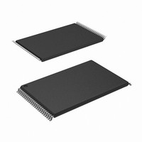
CY62167ELL-45ZXI Cypress Semiconductor Corp, CY62167ELL-45ZXI Datasheet - Page 4

CY62167ELL-45ZXI
Manufacturer Part Number
CY62167ELL-45ZXI
Description
CY62167ELL-45ZXI
Manufacturer
Cypress Semiconductor Corp
Datasheet
1.CY62167ELL-45ZXI.pdf
(15 pages)
Specifications of CY62167ELL-45ZXI
Format - Memory
RAM
Memory Type
SRAM
Memory Size
16M (2M x 8 or 1M x 16)
Speed
45ns
Interface
Parallel
Voltage - Supply
4.5 V ~ 5.5 V
Operating Temperature
-40°C ~ 85°C
Package / Case
48-TSOP I
Density
16Mb
Access Time (max)
45ns
Sync/async
Asynchronous
Architecture
SDR
Clock Freq (max)
Not RequiredMHz
Operating Supply Voltage (typ)
5V
Address Bus
21/20Bit
Package Type
TSOP-I
Operating Temp Range
-40C to 85C
Number Of Ports
1
Supply Current
30mA
Operating Supply Voltage (min)
4.5V
Operating Supply Voltage (max)
5.5V
Operating Temperature Classification
Industrial
Mounting
Surface Mount
Pin Count
48
Word Size
8/16Bit
Number Of Words
2M/1M
Lead Free Status / RoHS Status
Lead free / RoHS Compliant
Lead Free Status / RoHS Status
Lead free / RoHS Compliant
Available stocks
Company
Part Number
Manufacturer
Quantity
Price
Company:
Part Number:
CY62167ELL-45ZXI
Manufacturer:
CYPRESSRESS
Quantity:
5 530
Company:
Part Number:
CY62167ELL-45ZXI
Manufacturer:
CYP
Quantity:
3 586
Company:
Part Number:
CY62167ELL-45ZXI
Manufacturer:
CYPRESS
Quantity:
624
Part Number:
CY62167ELL-45ZXI
Manufacturer:
CYPRESS/赛普拉斯
Quantity:
20 000
Maximum Ratings
Exceeding maximum ratings may shorten the useful life of the
device. User guidelines are not tested.
Storage temperature ................................ –65 °C to +150 °C
Ambient temperature with
power applied ........................................... –55 °C to +125 °C
Supply voltage to ground
potential ..........................................................–0.5 V to 6.0 V
DC voltage applied to outputs
in high Z state
Electrical Characteristics
Over the Operating Range
Capacitance
Thermal Resistance
Notes
Document Number: 001-15607 Rev. *B
V
V
V
V
I
I
I
I
C
C
Parameter
Parameter
5. V
6. V
7. Full Device AC operation is based on a 100 µs ramp time from 0 to V
8. Under DC conditions the device meets a V
9. Typical values are included for reference only and are not guaranteed or tested. Typical values are measured at V
10. Chip enables (CE
11. Tested initially and after any design or process changes that may affect these parameters.
IX
OZ
CC
SB2
OH
OL
IH
IL
IN
OUT
Parameter
[10]
IL
IH
Θ
(min) = –2.0 V for pulse durations less than 20 ns.
Θ
(max) = V
JA
JC
[11]
[11]
CC
[5, 6]
Input capacitance
Output capacitance
Thermal resistance
(junction to ambient)
Thermal resistance
(junction to case)
+ 0.75 V for pulse durations less than 20 ns.
Output HIGH voltage
Output LOW voltage
Input HIGH voltage
Input LOW voltage
Input leakage current
Output leakage current
V
current
Automatic power down
current—CMOS inputs
1
CC
and CE
...........................................–0.5 V to 6.0 V
operating supply
2
Description
Description
Description
), byte enables (BHE and BLE) and BYTE need to be tied to CMOS levels to meet the I
IL
of 0.8 V. However, in dynamic conditions input LOW voltage applied to the device must not be higher than 0.7 V.
T
V
Still air, soldered on a 3 × 4.5 inch, two-layer printed circuit
board
I
I
V
V
GND < V
GND < V
f = f
f = 1 MHz
CE
and BLE > V
V
OH
OL
A
CC
CC
CC
IN
= 25 °C, f = 1 MHz,
1
= 2.1 mA
MAX
= –1.0 mA
< 0.2 V, f = 0, V
= V
= 4.5 V to 5.5 V
= 4.5 V to 5.5 V
> V
CC
CC
= 1/t
I
O
(typ)
< V
< V
CC
– 0.2 V or CE
CC
RC
(min) and 200 µs wait time after V
Test Conditions
CC
CC
– 0.2 V, V
, output disabled
CC
V
I
CMOS levels
OUT
Test Conditions
Test Conditions
DC input voltage
Output current into outputs (LOW) ............................. 20 mA
Static discharge voltage........................................... >2001 V
(MIL-STD-883, method 3015)
Latch-up current ...................................................... >200 mA
Operating Range
CC
CY62167ELL
= V
= V
2
IN
= 0 mA
CC
Device
< 0.2 V, or BHE
> V
CC
(max)
CC
(max)
– 0.2 V or
[5, 6]
CC
Industrial –40 °C to +85 °C 4.5 V to 5.5 V
Range
stabilization.
.......................................–0.5 V to 6.0 V
SB2
CC
–0.5
/ I
Min
2.4
2.2
–1
–1
= V
CCDR
–
–
–
–
CC
Temperature
(typ), T
spec. Other inputs can be left floating.
Ambient
CY62167E MoBL
Typ
2.2
1.5
25
45 ns
–
–
–
–
–
–
A
[9]
= 25 °C
TSOP I
Max
V
4.3
10
10
60
CC
0.7
Max
0.4
4.0
+ 0.5 V
+1
+1
12
30
–
[8]
Page 4 of 15
V
CC
°C/W
°C/W
Unit
Unit
pF
pF
[7]
Unit
mA
mA
µA
µA
µA
V
V
V
V
®
[+] Feedback


