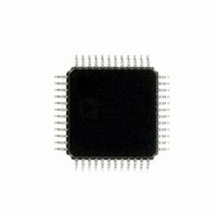
ADUC7060BSTZ32 Analog Devices Inc, ADUC7060BSTZ32 Datasheet - Page 19

ADUC7060BSTZ32
Manufacturer Part Number
ADUC7060BSTZ32
Description
DUAL 24-BIT AFE AND ARM 7 I.C
Manufacturer
Analog Devices Inc
Series
MicroConverter® ADuC7xxxr
Specifications of ADUC7060BSTZ32
Design Resources
4 mA-to-20 mA Loop-Powered Temperature Monitor Using ADuC7060/1 (CN0145) Low power, Long Range, ISM Wireless Measuring Node (CN0164)
Core Processor
ARM7
Core Size
16/32-Bit
Speed
10MHz
Connectivity
I²C, SPI, UART/USART
Peripherals
POR, PWM, Temp Sensor, WDT
Number Of I /o
14
Program Memory Size
32KB (16K x 16)
Program Memory Type
FLASH
Ram Size
4K x 8
Voltage - Supply (vcc/vdd)
2.375 V ~ 2.625 V
Data Converters
A/D 5x24b, 8x24b, D/A 1x14b
Oscillator Type
Internal
Operating Temperature
-40°C ~ 125°C
Package / Case
48-LQFP
Cpu Family
ADuC7xxx
Device Core
ARM7TDMI
Device Core Size
16/32Bit
Frequency (max)
10.24MHz
Interface Type
I2C/SPI/UART
Total Internal Ram Size
4KB
# I/os (max)
14
Number Of Timers - General Purpose
4
Operating Supply Voltage (typ)
2.5V
Operating Supply Voltage (max)
2.625V
Operating Supply Voltage (min)
2.375V
On-chip Adc
2(4-chx24-bit)
Instruction Set Architecture
RISC
Operating Temp Range
-40C to 125C
Operating Temperature Classification
Automotive
Mounting
Surface Mount
Pin Count
48
Package Type
LQFP
Package
48LQFP
Family Name
ADuC7xxx
Maximum Speed
10.24 MHz
Operating Supply Voltage
2.5 V
Data Bus Width
16|32 Bit
Number Of Programmable I/os
14
Number Of Timers
4
Lead Free Status / RoHS Status
Lead free / RoHS Compliant
Eeprom Size
-
Lead Free Status / Rohs Status
Compliant
Available stocks
Company
Part Number
Manufacturer
Quantity
Price
Company:
Part Number:
ADUC7060BSTZ32
Manufacturer:
CYPRESS
Quantity:
294
Company:
Part Number:
ADUC7060BSTZ32
Manufacturer:
ADI
Quantity:
315
Company:
Part Number:
ADUC7060BSTZ32
Manufacturer:
Analog Devices Inc
Quantity:
10 000
Part Number:
ADUC7060BSTZ32
Manufacturer:
ADI/亚德诺
Quantity:
20 000
Company:
Part Number:
ADUC7060BSTZ32-RL
Manufacturer:
Analog Devices Inc
Quantity:
10 000
Pin No.
21
22
23
24
25
26
27
28
29
30
31
32
1
I = input, O = output, I/O = input/output, and S = supply.
Mnemonic
P0.2/MISO/ADC8
P0.3/MOSI/SDA/ADC9
XTALO
XTALI
P0.4/IRQ0/PWM1
P2.0/IRQ2/PWM0
DGND
DVDD
NTRST/BM
TDO
TDI
TCK
I/O
I/O
I/O
I/O
S
S
O
Type
O
I
I
I
I
1
Description
General-Purpose Input and General-Purpose Output P0.2/SPI Master Input Slave
Output/Auxiliary ADC8 Input. This is a triple function input/output pin. Single-ended or
differential Analog Input 8. Analog input for the auxiliary ADC.
General-Purpose Input and General-Purpose Output P0.3/SPI Master Output Slave Input/I
Data Pin/Auxiliary ADC9 Input. This is a multifunction input/output pin. Single-ended or
differential Analog Input 9. Analog input for the auxiliary ADC.
External Crystal Oscillator Output Pin.
External Crystal Oscillator Input Pin.
General-Purpose Input and General-Purpose Output P0.4/External Interrupt Request 0/PWM1
Output. This is a triple function input/output pin.
General-Purpose Input and General-Purpose Output P2.0/External Interrupt Request 2/PWM0
Output. This is a triple function input/output pin.
Digital Ground.
Digital Supply Pin.
JTAG Reset/Boot Mode. Input pin used for debug and download only and boot mode (BM). The
ADuC7061 enters serial download mode if BM is low at reset and executes code if BM is pulled
high at reset through a 13 kΩ resistor.
JTAG Data Out. Output pin used for debug and download only.
JTAG Data In. Input pin used for debug and download only. Add an external pull-up resistor
(~100 kΩ) to this pin.
JTAG Clock. Input pin used for debug and download only. Add an external pull-up resistor
(~100 kΩ) to this pin.
Rev. C | Page 19 of 108
ADuC7060/ADuC7061
2
C


