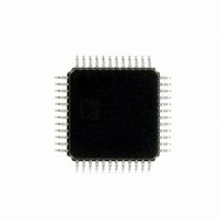
ADUC7060BSTZ32 Analog Devices Inc, ADUC7060BSTZ32 Datasheet - Page 102

ADUC7060BSTZ32
Manufacturer Part Number
ADUC7060BSTZ32
Description
DUAL 24-BIT AFE AND ARM 7 I.C
Manufacturer
Analog Devices Inc
Series
MicroConverter® ADuC7xxxr
Specifications of ADUC7060BSTZ32
Design Resources
4 mA-to-20 mA Loop-Powered Temperature Monitor Using ADuC7060/1 (CN0145) Low power, Long Range, ISM Wireless Measuring Node (CN0164)
Core Processor
ARM7
Core Size
16/32-Bit
Speed
10MHz
Connectivity
I²C, SPI, UART/USART
Peripherals
POR, PWM, Temp Sensor, WDT
Number Of I /o
14
Program Memory Size
32KB (16K x 16)
Program Memory Type
FLASH
Ram Size
4K x 8
Voltage - Supply (vcc/vdd)
2.375 V ~ 2.625 V
Data Converters
A/D 5x24b, 8x24b, D/A 1x14b
Oscillator Type
Internal
Operating Temperature
-40°C ~ 125°C
Package / Case
48-LQFP
Cpu Family
ADuC7xxx
Device Core
ARM7TDMI
Device Core Size
16/32Bit
Frequency (max)
10.24MHz
Interface Type
I2C/SPI/UART
Total Internal Ram Size
4KB
# I/os (max)
14
Number Of Timers - General Purpose
4
Operating Supply Voltage (typ)
2.5V
Operating Supply Voltage (max)
2.625V
Operating Supply Voltage (min)
2.375V
On-chip Adc
2(4-chx24-bit)
Instruction Set Architecture
RISC
Operating Temp Range
-40C to 125C
Operating Temperature Classification
Automotive
Mounting
Surface Mount
Pin Count
48
Package Type
LQFP
Package
48LQFP
Family Name
ADuC7xxx
Maximum Speed
10.24 MHz
Operating Supply Voltage
2.5 V
Data Bus Width
16|32 Bit
Number Of Programmable I/os
14
Number Of Timers
4
Lead Free Status / RoHS Status
Lead free / RoHS Compliant
Eeprom Size
-
Lead Free Status / Rohs Status
Compliant
Available stocks
Company
Part Number
Manufacturer
Quantity
Price
Company:
Part Number:
ADUC7060BSTZ32
Manufacturer:
CYPRESS
Quantity:
294
Company:
Part Number:
ADUC7060BSTZ32
Manufacturer:
ADI
Quantity:
315
Company:
Part Number:
ADUC7060BSTZ32
Manufacturer:
Analog Devices Inc
Quantity:
10 000
Part Number:
ADUC7060BSTZ32
Manufacturer:
ADI/亚德诺
Quantity:
20 000
Company:
Part Number:
ADUC7060BSTZ32-RL
Manufacturer:
Analog Devices Inc
Quantity:
10 000
ADuC7060/ADuC7061
Table 110. GPxCON MMR Bit Designations
Bit
31:30
29:28
27:26
25:24
23:22
21:20
19:18
17:16
15:14
13:12
11:10
9:8
7:6
5:4
3:2
1:0
GPxDAT REGISTERS
GPxDAT are Port x configuration and data registers. They con-
figure the direction of the GPIO pins of Port x, set the output
value for the pins that are configured as output, and store the
input value of the pins that are configured as input.
Table 111. GPxDAT Registers
Name
GP0DAT
GP1DAT
GP2DAT
Table 112. GPxDAT MMR Bit Designations
Bit
31:24
23:16
15:8
7:0
Description
Reserved.
Reserved.
Reserved.
Selects the function of the P0.6/RTS and P1.6/PWM pins.
Reserved.
Selects the function of the P0.5/CTS and P1.5/PWM3 pins.
Reserved.
Selects the function of the P0.4/IRQ0/PWM1 and
P1.4/PWM2 pins.
Reserved.
Selects the function of the P0.3/MOSI/SDA and P1.3/TRIP
pins.
Reserved.
Selects the function of the P0.2/MISO and P1.2/SYNC pins.
Reserved.
Selects the function of the P0.1/SCLK/SCL, P1.1/SOUT,
and P2.1/IRQ3/PWM5 pins.
Reserved.
Selects the function of the P0.0/SS, P1.0/IRQ1/SIN/T0,
P2.0/IRQ2/PWM0/EXTCLK pins.
Description
Direction of the data.
Set to 1 by user to configure the GPIO pin as an output.
Cleared to 0 by user to configure the GPIO pin as an input.
Port x data output.
Reflect the state of Port x pins at reset (read only).
Port x data input (read only).
Address
0xFFFF0D20
0xFFFF0D30
0xFFFF0D40
Default Value
0x000000XX
0x000000XX
0x000000XX
Access
R/W
R/W
R/W
Rev. C | Page 102 of 108
GPxSET REGISTERS
GPxSET are data set Port x registers.
Table 113. GPxSET Registers
Name
GP0SET
GP1SET
GP2SET
Table 114. GPxSET MMR Bit Designations
Bit
31:24
23:16
15:0
GPxCLR REGISTERS
GPxCLR are data clear Port x registers.
Table 115. GPxCLR Registers
Name
GP0CLR
GP1CLR
GP2CLR
Table 116. GPxCLR MMR Bit Designations
Bit
31:24
23:16
15:0
GPxPAR REGISTERS
The GPxPAR registers program the parameters for Port 0, Port 1,
and Port 2. Note that the GPxDAT MMR must always be written
after changing the GPxPAR MMR. Note that it is not possible to
disable the internal pull-up resistor on P0.2.
Table 117. GPxPAR Registers
Name
GP0PAR
GP1PAR
GP2PAR
Description
Reserved.
Data Port x set bit.
Set to 1 by user to set bit on Port x; also sets the
corresponding bit in the GPxDAT MMR.
Cleared to 0 by user; does not affect the data output.
Reserved.
Description
Reserved.
Data Port x clear bit.
Reserved.
Set to 1 by user to clear the bit on Port x; also clears
the corresponding bit in the GPxDAT MMR.
Cleared to 0 by user; does not affect the data output.
Address
0xFFFF0D28
0xFFFF0D38
0xFFFF0D48
Address
0xFFFF0D24
0xFFFF0D34
0xFFFF0D44
Address
0xFFFF0D2C
0xFFFF0D3C
0xFFFF0D4C
Default Value
0x000000XX
0x000000XX
0x000000XX
Default Value
0x000000XX
0x000000XX
0x000000XX
Default Value
0x00000000
0x00000000
0x00000000
Access
W
W
W
Access
W
W
W
Access
R/W
R/W
R/W


