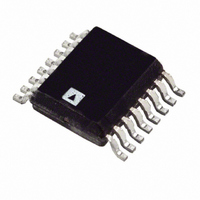
ADT7470ARQZ-REEL Analog Devices Inc, ADT7470ARQZ-REEL Datasheet - Page 38

ADT7470ARQZ-REEL
Manufacturer Part Number
ADT7470ARQZ-REEL
Description
IC,Motor Controller,SSOP,16PIN
Manufacturer
Analog Devices Inc
Datasheet
1.ADT7470ARQZ.pdf
(40 pages)
Specifications of ADT7470ARQZ-REEL
Function
Fan Control, Temp Monitor
Topology
ADC, Comparator, Fan Speed Control, Register Bank
Sensor Type
External
Sensing Temperature
External Sensor
Output Type
I²C™
Output Alarm
No
Output Fan
Yes
Voltage - Supply
3 V ~ 5.5 V
Operating Temperature
-40°C ~ 125°C
Mounting Type
Surface Mount
Package / Case
16-QSOP
Lead Free Status / RoHS Status
Lead free / RoHS Compliant
For Use With
EVAL-ADT7470EBZ - BOARD EVALUATION FOR ADT7470
Lead Free Status / RoHS Status
Lead free / RoHS Compliant
Available stocks
Company
Part Number
Manufacturer
Quantity
Price
Part Number:
ADT7470ARQZ-REEL7
Manufacturer:
ADI/亚德诺
Quantity:
20 000
ADT7470
Table 49. Register 0x80. GPIO CONFIG (Power-On Default = 0x00).
Bit Name
[7] GPIO1_d
[6] GPIO1_p
[5] GPIO2_d
[4] GPIO2_p
[3] GPIO3_d
[2] GPIO3_p
[1] GPIO4_d
[0] GPIO4_p
Table 50. Register 0x81. GPIO Status (Power-On Default = 0x00).
Bit Name
[7:4] GPIO_s
[7] GPIO4_s
[6] GPIO3_s
[5] GPIO2_s
[4] GPIO1_s
[3:0] Reserved
Read/Write
Read/Write
Read/Write
Read/Write
Read/Write
Read/Write
Read/Write
Read/Write
Read/Write
Read/Write
Read/Write
Read/Write
Read/Write
Read/Write
Read/Write
Read/Write
Description
This bit sets the direction of GPIO 1 when the PWM1 pin is configured as GPIO.
1= output; 0 = input.
Data for GPIO 1 is set by the LSB of the PWM1 min duty cycle register.
This bit sets the polarity of GPIO 1 when the PWM1 pin is configured as GPIO.
1 = active high; 0 = active low.
This bit sets the direction of GPIO 2 when the PWM2 pin is configured as GPIO.
1= output; 0 = input.
Data for GPIO 2 is set by the LSB of the PWM2 min duty cycle register.
This bit sets the polarity of GPIO 2 when the PWM2 pin is configured as GPIO.
1 = active high; 0 = active low.
This bit sets the direction of GPIO 3 when the PWM3 pin is configured as GPIO.
1= output; 0 = input.
Data for GPIO 3 is set by the LSB of the PWM3 min duty cycle register.
This bit sets the polarity of GPIO 3 when the PWM3 pin is configured as GPIO.
1 = active high; 0 = active low.
This bit sets the direction of GPIO 4 when the PWM4 pin is configured as GPIO.
1= output; 0 = input.
Data for GPIO 4 is set by the LSB of the PWM4 min duty cycle register.
This bit sets the polarity of GPIO 4 when the PWM4 pin is configured as GPIO.
1 = active high; 0 = active low.
Description
These bits indicate the status of the GPIO when the corresponding PWM pin is configured
as GPIO.
When GPIO is configured as an input, these bits are read-only. They are set when the input
is asserted. (Asserted can be high or low depending on the setting of the GPIO polarity.)
When GPIO is configured as an output, these bits are read/write. Setting these bits asserts
the GPIO output. (Asserted can be high or low depending on the setting of GPIO4
polarity.)
This bit indicates the status of GPIO 4 when the PWM4 pin is configured as GPIO.
This bit indicates the status of GPIO 3 when the PWM3 pin is configured as GPIO.
This bit indicates the status of GPIO 2 when the PWM2 pin is configured as GPIO.
This bit indicates the status of GPIO 1 when the PWM1 pin is configured as GPIO.
Test Bit. For Analog Devices use only.
Rev. C | Page 38 of 40


