ADSP-21160MKB-80 Analog Devices Inc, ADSP-21160MKB-80 Datasheet - Page 4
ADSP-21160MKB-80
Manufacturer Part Number
ADSP-21160MKB-80
Description
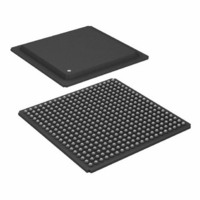
IC,DSP,32-BIT,CMOS,BGA,400PIN,PLASTIC
Manufacturer
Analog Devices Inc
Series
SHARC®r
Type
Floating Pointr
Datasheet
1.ADSP-21160MKBZ-80.pdf
(52 pages)
Specifications of ADSP-21160MKB-80
Rohs Compliant
NO
Rohs Status
RoHS non-compliant
Interface
Host Interface, Link Port, Serial Port
Clock Rate
80MHz
Non-volatile Memory
External
On-chip Ram
512kB
Voltage - I/o
3.30V
Voltage - Core
2.50V
Operating Temperature
0°C ~ 85°C
Mounting Type
Surface Mount
Package / Case
400-BGA
Lead Free Status / RoHS Status
Available stocks
Company
Part Number
Manufacturer
Quantity
Price
Company:

Part Number:
ADSP-21160MKB-80
Manufacturer:
AD
Quantity:
1 831
Company:
Part Number:
ADSP-21160MKB-80
Manufacturer:
Analog Devices Inc
Quantity:
10 000


ADSP-21160M
With the ADSP-21160M’s separate program and data
memory buses and on-chip instruction cache, the processor
can simultaneously fetch four operands and an instruction
(from the cache), all in a single cycle.
Instruction Cache
The ADSP-21160M includes an on-chip instruction cache
that enables three-bus operation for fetching an instruction
and four data values. The cache is selective—only the
instructions whose fetches conflict with PM bus data
accesses are cached. This cache allows full-speed execution
of core, providing looped operations such as digital filter
multiply- accumulates and FFT butterfly processing.
Data Address Generators with Hardware
Circular Buffers
The ADSP-21160M’s two data address generators (DAGs)
are used for indirect addressing and provide for implement-
ing circular data buffers in hardware. Circular buffers allow
efficient programming of delay lines and other data struc-
tures required in digital signal processing, and are
commonly used in digital filters and Fourier transforms.
The two DAGs of the ADSP-21160M contain sufficient
registers to allow the creation of up to 32 circular buffers
(16 primary register sets, 16 secondary). The DAGs auto-
matically handle address pointer wraparound, reducing
overhead, increasing performance, and simplifying imple-
mentation. Circular buffers can start and end at any
memory location.
Flexible Instruction Set
The 48-bit instruction word accommodates a variety of
parallel operations, for concise programming. For example,
the ADSP-21160M can conditionally execute a multiply, an
add, and subtract, in both processing elements, while
branching, all in a single instruction.
ADSP-21160M Memory and I/O Interface Features
Augmenting the ADSP-2116x family core, the
ADSP-21160M adds the following architectural features:
Dual-Ported On-Chip Memory
The ADSP-21160M contains four megabits of on-chip
SRAM, organized as two blocks of 2 Mbits each, which can
be configured for different combinations of code and data
storage. Each memory block is dual-ported for single-cycle,
independent accesses by the core processor and I/O proces-
sor. The dual-ported memory in combination with three
separate on-chip buses allows two data transfers from the
core and one from I/O processor, in a single cycle. On the
ADSP-21160M, the memory can be configured as a
maximum of 128K words of 32-bit data, 256K words of
16-bit data, 85K words of 48-bit instructions (or 40-bit
data), or combinations of different word sizes up to four
megabits. All of the memory can be accessed as 16-bit,
32-bit, 48-bit, or 64-bit words. A 16-bit floating-point
storage format is supported that effectively doubles the
amount of data that may be stored on-chip. Conversion
–4–
between the 32-bit floating-point and 16-bit floating-point
formats is done in a single instruction. While each memory
block can store combinations of code and data, accesses are
most efficient when one block stores data, using the DM
bus for transfers, and the other block stores instructions and
data, using the PM bus for transfers. Using the DM bus and
PM bus in this way, with one dedicated to each memory
block, assures single-cycle execution with two data trans-
fers. In this case, the instruction must be available in
the cache.
Off-Chip Memory and Peripherals Interface
The ADSP-21160M’s external port provides the proces-
sor’s interface to off-chip memory and peripherals. The
4G word off-chip address space is included in the
ADSP-21160M’s unified address space. The separate
on-chip buses—for PM addresses, PM data, DM addresses,
DM data, I/O addresses, and I/O data—are multiplexed at
the external port to create an external system bus with a
single 32-bit address bus and a single 64-bit data bus. The
lower 32 bits of the external data bus connect to even
addresses and the upper 32 bits of the 64 connect to odd
addresses. Every access to external memory is based on an
address that fetches a 32-bit word, and with the 64-bit bus,
two address locations can be accessed at once. When
fetching an instruction from external memory, two 32-bit
data locations are being accessed (16 bits are unused).
Figure 3
external memory.
The external port supports asynchronous, synchronous,
and synchronous burst accesses. ZBT synchronous burst
SRAM can be interfaced gluelessly. Addressing of external
memory devices is facilitated by on-chip decoding of
high-order address lines to generate memory bank select
signals. Separate control lines are also generated for simpli-
fied addressing of page-mode DRAM. The ADSP-21160M
provides programmable memory wait states and external
memory acknowledge controls to allow interfacing to
DRAM and peripherals with variable access, hold, and
disable time requirements.
DMA Controller
The ADSP-21160M’s on-chip DMA controller allows
zero-overhead data transfers without processor interven-
tion. The DMA controller operates independently and
invisibly to the processor core, allowing DMA operations to
occur while the core is simultaneously executing its program
instructions. DMA transfers can occur between the
ADSP-21160M’s internal memory and external memory,
external peripherals, or a host processor. DMA transfers can
also occur between the ADSP-21160M’s internal memory
and its serial ports or link ports. External bus packing to
16-, 32-, 48-, or 64-bit words is performed during DMA
transfers. Fourteen channels of DMA are available on the
ADSP-21160M—six via the link ports, four via the serial
ports, and four via the processor’s external port (for either
shows the alignment of various accesses to
REV. 0
Related parts for ADSP-21160MKB-80
Image
Part Number
Description
Manufacturer
Datasheet
Request
R

Part Number:
Description:
±1.7g Dual-Axis IMEMS Accelerometer Evaluation Board
Manufacturer:
Analog Devices Inc
Datasheet:

Part Number:
Description:
Inertial Sensor Evaluation System
Manufacturer:
Analog Devices Inc
Datasheet:
Part Number:
Description:
Manufacturer:
Analog Devices Inc
Datasheet:
Part Number:
Description:
Manufacturer:
Analog Devices Inc
Datasheet:
Part Number:
Description:
Manufacturer:
Analog Devices Inc
Datasheet:
Part Number:
Description:
Manufacturer:
Analog Devices Inc
Datasheet:
Part Number:
Description:
Manufacturer:
Analog Devices Inc
Datasheet:
Part Number:
Description:
Manufacturer:
Analog Devices Inc
Datasheet:
Part Number:
Description:
Manufacturer:
Analog Devices Inc
Datasheet:
Part Number:
Description:
Manufacturer:
Analog Devices Inc
Datasheet:
Part Number:
Description:
Manufacturer:
Analog Devices Inc
Datasheet:
Part Number:
Description:
Manufacturer:
Analog Devices Inc
Datasheet:
Part Number:
Description:
Manufacturer:
Analog Devices Inc
Datasheet: