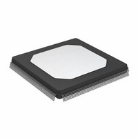
ADSP-21060KS-160 Analog Devices Inc, ADSP-21060KS-160 Datasheet - Page 40

ADSP-21060KS-160
Manufacturer Part Number
ADSP-21060KS-160
Description
Digital Signal Processor IC
Manufacturer
Analog Devices Inc
Series
SHARC®r
Type
Floating Pointr
Datasheets
1.ADSP-21062KSZ-133.pdf
(64 pages)
2.ADSP-21060KS-160.pdf
(47 pages)
3.ADSP-21060KS-160.pdf
(64 pages)
Specifications of ADSP-21060KS-160
Supply Voltage Max
5.25V
Dsp Type
Fixed / Floating Point
Mounting Type
Surface Mount
Package / Case
240-MQFP
Memory Organization - Ram
4M
Rohs Status
RoHS non-compliant
Interface
Host Interface, Link Port, Serial Port
Clock Rate
40MHz
Non-volatile Memory
External
On-chip Ram
512kB
Voltage - I/o
5.00V
Voltage - Core
5.00V
Operating Temperature
0°C ~ 85°C
Device Core Size
32b
Architecture
Super Harvard
Format
Floating Point
Clock Freq (max)
40MHz
Mips
40
Device Input Clock Speed
40MHz
Ram Size
512KB
Operating Supply Voltage (typ)
5V
Operating Supply Voltage (min)
4.75V
Operating Supply Voltage (max)
5.25V
Operating Temp Range
0C to 85C
Operating Temperature Classification
Commercial
Mounting
Surface Mount
Pin Count
240
Package Type
MQFP
Lead Free Status / Rohs Status
Not Compliant
Available stocks
Company
Part Number
Manufacturer
Quantity
Price
Company:
Part Number:
ADSP-21060KS-160
Manufacturer:
AD
Quantity:
5 510
Company:
Part Number:
ADSP-21060KS-160
Manufacturer:
SHARP
Quantity:
5 510
Company:
Part Number:
ADSP-21060KS-160
Manufacturer:
Analog Devices Inc
Quantity:
10 000
Example System Hold Time Calculation
To determine the data output hold time in a particular system,
first calculate t
to be the difference between the ADSP-2106x’s output voltage
and the input threshold for the device requiring the hold time. A
typical ∆V will be 0.4 V. C
data line), and I
data line). The hold time will be t
disable time (i.e., t
ADSP-21060/ADSP-21060L
REFERENCE
V
V
OH (MEASURED)
OL (MEASURED)
SIGNAL
t
DIS
OUTPUT STOPS
DECAY
L
DRIVING
is the total leakage or three-state current (per
DATRWH
using the equation given above. Choose ∆V
t
MEASURED
V
V
OH (MEASURED)
OL (MEASURED)
t
DECAY
L
for the write cycle).
is the total bus capacitance (per
HIGH-IMPEDANCE STATE.
TEST CONDITIONS CAUSE
THIS VOLTAGE TO BE
APPROXIMATELY 1.5V
DECAY
+ V
– V
OUTPUT STARTS
plus the minimum
t
ENA
1.0V
2.0V
DRIVING
V
V
OH (MEASURED)
OL (MEASURED)
Capacitive Loading
Output delays and holds are based on standard capacitive loads:
50 pF on all pins (see Figure 26). The delay and hold specifica-
tions given should be derated by a factor of 1.5 ns/50 pF for
loads other than the nominal value of 50 pF. Figures 29–30,
33–34 show how output rise time varies with capacitance. Fig-
ures 31, 35 show graphically how output delays and holds vary
with load capacitance. (Note that this graph or derating does
not apply to output disable delays; see the previous section
Output Disable Time under Test Conditions.) The graphs of
Figures 29, 30 and 31 may not be linear outside the ranges
shown.
OUTPUT
INPUT OR
PIN
OUTPUT
TO
50pF
1.5V
I
I
OH
OL
+1.5V
1.5V


