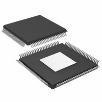
AD9778ABSVZ Analog Devices Inc, AD9778ABSVZ Datasheet - Page 46

AD9778ABSVZ
Manufacturer Part Number
AD9778ABSVZ
Description
IC,D/A CONVERTER,DUAL,14-BIT,CMOS,TQFP,100PIN
Manufacturer
Analog Devices Inc
Specifications of AD9778ABSVZ
Number Of Bits
14
Data Interface
Parallel
Number Of Converters
2
Voltage Supply Source
Analog and Digital
Power Dissipation (max)
300mW
Operating Temperature
-40°C ~ 85°C
Mounting Type
Surface Mount
Package / Case
100-TQFP Exposed Pad, 100-eTQFP, 100-HTQFP, 100-VQFP
Package
100TQFP EP
Resolution
14 Bit
Conversion Rate
1 GSPS
Architecture
Interpolation Filter
Digital Interface Type
Parallel
Number Of Outputs Per Chip
2
Output Type
Current
Full Scale Error
±2(Typ) %FSR
Integral Nonlinearity Error
±1.5(Typ) LSB
Lead Free Status / RoHS Status
Lead free / RoHS Compliant
For Use With
AD9778A-EBZ - BOARD EVALUATION AD9778A
Settling Time
-
Lead Free Status / RoHS Status
Lead free / RoHS Compliant
Available stocks
Company
Part Number
Manufacturer
Quantity
Price
Company:
Part Number:
AD9778ABSVZ
Manufacturer:
Analog Devices Inc
Quantity:
135
Company:
Part Number:
AD9778ABSVZ
Manufacturer:
Analog Devices Inc
Quantity:
10 000
Part Number:
AD9778ABSVZ
Manufacturer:
ADI/亚德诺
Quantity:
20 000
Company:
Part Number:
AD9778ABSVZRL
Manufacturer:
Analog Devices Inc
Quantity:
10 000
AD9776A/AD9778A/AD9779A
INPUT DATA PORTS
The AD9776A/AD9778A/AD9779A can operate in two data
input modes: dual port mode and single port mode. For the
default dual port mode (single port bit = 0), each DAC receives
data from a dedicated input port. In single port mode (single
port bit = 1), both DACs receive data from Port 1. In single port
mode, DAC1 and DAC2 data is interleaved, and the TXENABLE
input is used to steer data to the intended DAC. In dual port
mode, the TXENABLE input is used to power down the digital
data path.
In dual port mode, the data must be delivered at the input data
rate. In single port mode, data must be delivered at twice the
input data rate of each DAC. Because the data inputs function
up to a maximum of 300 MSPS, it is practical to operate with
input data rates up to 150 MHz per DAC in single port mode.
In dual port and single port modes, a data clock output
(DATACLK) signal is available as a fixed time base with which
to drive data from an FPGA or other data source. This output
signal operates at the input data rate.
SINGLE PORT MODE
In single port mode, data for both DACs is received on the Port 1
input bus (P1D[15:0]). I and Q data samples are interleaved and
are sampled on the rising edges of DATACLK. Along with the
data, a framing signal must be supplied on the TXENABLE
input (Pin 39), which steers incoming data to its respective DAC.
When TXENABLE is high, the corresponding data-word is sent
to the I DAC. When TXENABLE is low, the corresponding data is
sent to the Q DAC. The timing of the digital interface in
interleaved mode is shown in Figure 83.
The Q first bit (Register 0x02, Bit 0) controls the pairing order
of the input data. With the Q first bit set to the default of 0, the
I-Q pairing sent to the DACs is the two input data-words
corresponding to TXENABLE low followed by TXENABLE
high. With the Q first bit set to 1, the I-Q pairing sent to the
DACs is the two input data-words corresponding to TXENABLE
high, followed by TXENABLE low. Note that with either order
pairing, the data sent with TXENABLE high is directed to the
I DAC, and the data sent with TXENABLE low is directed to the
Q DAC.
Q FIRST = 0
Q FIRST = 1
Q DAC[15:0]
Q DAC[15:0]
TXENABLE
I DAC[15:0]
I DAC[15:0]
DATACLK
P1D[15:0]
Figure 83. Single Port Mode Digital Interface Timing
P1D1
Rev. B | Page 46 of 56
P1D2
P1D3
P1D4
P1D1
P1D2
P1D1
P1D0
DUAL PORT MODE
In dual port mode, data for each DAC is received on the
respective input bus (P1D[15:0] or P2D[15:0]). I and Q data
arrive simultaneously and are sampled on the rising edge of the
DATACLK signal. The TXENABLE signal must be high to enable
the transmit path.
INPUT DATA REFERENCED TO DATACLK
The simplest method of interfacing to the AD9776A/AD9778A/
AD9779A is when the input data is referenced to the DATACLK
output. The DATACLK output is a buffered version (with some
fixed delay) of the internal clock that is used to latch the input
data. Therefore, if setup and hold times of the input data with
respect to DATACLK are met, the input data is latched correctly.
Detailed timing diagrams for the single and dual port cases
using DATACLK as the timing reference are shown in Figure 82.
Table 28 shows the setup and hold time requirements for the
input data over the operating temperature range of the device.
Also shown is the keep out window (KOW). The keep out
window is the sum of the setup and hold times of the interface.
This is the minimum amount of time valid data must be
presented to the device to ensure proper sampling.
DATACLK Frequency Settings
The DATACLK signal is derived from the internal DAC sample
clock, DACCLK. The frequency of the DATACLK output depends
on several programmable settings. Normally, the frequency of
DATACLK is equal to the input data rate. The relationship
between the frequency of DACCLK and DATACLK is
where the variables IF, ZS, SP, and DATACLKDIV have the
values shown in Table 27.
DATACLK
DATA
P1D5
Figure 82. Input Data Port Timing, Data Referenced to DATACLK
f
DATACLK
P1D6
P1D3
P1D4
P1D3
P1D2
=
P1D7
IF
×
ZS
P1D8
P1D5
P1D6
P1D5
P1D4
×
SP
t
SDATACLK
f
DACCLK
×
DATACLKDIV
t
HDATACLK


