AD678KD Analog Devices Inc, AD678KD Datasheet - Page 6
AD678KD
Manufacturer Part Number
AD678KD
Description
A/D Converter (A-D) IC
Manufacturer
Analog Devices Inc
Datasheet
1.AD678JNZ.pdf
(14 pages)
Specifications of AD678KD
No. Of Bits
12 Bit
Mounting Type
Through Hole
Features
BiMOS, High-Impedance/-Bandwidth, 10V, AC/DC
No. Of Channels
1
Interface Type
Parallel
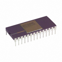
Package / Case
28-CDIP
Rohs Status
RoHS non-compliant
Number Of Bits
12
Sampling Rate (per Second)
200k
Data Interface
Parallel
Number Of Converters
2
Power Dissipation (max)
745mw
Voltage Supply Source
Analog and Digital, Dual ±
Operating Temperature
0°C ~ 70°C
Lead Free Status / RoHS Status
Available stocks
Company
Part Number
Manufacturer
Quantity
Price

Part Number:
AD678KD
Manufacturer:
ADI/亚德诺
Quantity:
20 000


AD678
Symbol
AGND
AIN
BIPOFF
CS
DGND
DB11–DB4
DB3, DB2
DB1 (R/L)
DB0 (HBE)
EOC
EOCEN
HBE (DB0)
OE
REF
REF
R/L (DB1)
SC
SYNC
V
V
V
12/8
No Connect
Type: AI = Analog Input; AO = Analog Output; DI = Digital Input (TTL and 5 V CMOS compatible); DO = Digital Output (TTL and 5 V CMOS compatible).
All DO pins are three-state drivers; P = Power.
CC
EE
DD
IN
OUT
28-Lead DIP 44-Lead
Pin No.
7
6
10
4
14
26–19
18, 17
16
15
27
1
15
2
9
8
16
3
13
11
5
28
12
REF
BIPOFF
EOCEN
AGND
DGND
REF
SYNC
12/8
V
AIN
V
OUT
OE
SC
CS
EE
CC
DIP PACKAGE
IN
10
11
12
13
14
1
2
3
4
5
6
7
8
9
(Not to Scale)
TOP VIEW
AD678
JLCC Pin No. Type
11
10
15
6
23
40, 39, 37, 36, DO
35, 34, 33, 31
30, 27
26
25
42
1
25
3
14
12
26
5
21
17
8
43
19
2, 4, 7, 9, 13,
16, 18, 20, 22,
24, 28, 29, 32,
38, 41, 44
19
18
17
16
15
28
27
26
25
24
23
22
21
20
V
EOC
DB11
DB10
DB9
DB8
DB7
DB6
DB5
DB4
DB3
DB2
DB1 (R/L)
DB0 (HBE)
DD
P
AI
AI
DI
P
DO
DO
DO
DO
DI
DI
DI
AI
AO
DI
DI
DI
P
P
P
DI
Name and Function
Analog Ground. This is the ground return for AIN only.
Analog Signal Input.
Bipolar Offset. Connect to AGND for +10 V input unipolar mode and straight binary
output coding. Connect to REF
and twos complement binary output coding. See Figures 7 and 8.
Chip Select. Active LOW.
Digital Ground
Data Bits 11 through 4. In 12-bit format (see 12/8 pin), these pins provide the upper 8 bits
of data. In 8-bit format, these pins provide all 12 bits in two bytes (see R/L pin).
Active HIGH.
Data Bits 3 and 2. In 12-bit format, these pins provide Data Bit 3 and Data Bit 2.
Active HIGH. In 8-bit format they are undefined and should be tied to V
In 12-bit format, Data Bit 1. Active HIGH.
In 12-bit format, Data Bit 0. Active HIGH.
End-of-Convert. EOC goes LOW when a conversion starts and goes HIGH when the
conversion is finished. In asynchronous mode, EOC is an open drain output and
requires an external 3 kΩ pull-up resistor. See EOCEN and SYNC pins for information
on EOC gating.
End-Of-Convert Enable. Enables EOC pin. Active LOW.
In 8-bit format, High Byte Enable. If LOW, output contains high byte. If HIGH, output
contains low byte.
Output Enable. The falling edge of OE enables DB11–DB0 in 12-bit format and
DB11–DB4 in 8-bit format. Gated with CS. Active LOW.
Reference Input. +5 V input gives 10 V full-scale range.
+5 V Reference Output. Tied to REF
In 8-bit format, Right/Left justified. Sets alignment of 12-bit result within 16-bit field.
Tied to V
Start Convert. Active LOW. See SYNC pin for gating.
SYNC Control. If tied to V
by CS. If tied to DGND (asynchronous mode), SC and EOCEN are independent of CS,
and EOC is an open drain output. EOC requires an external 3 kΩ pull-up resistor in
asynchronous mode.
+12 V Analog Power.
–12 V Analog Power.
+5 V Digital Power.
Twelve/eight-bit format. If tied HIGH, sets output format to 12-bit parallel. If tied
LOW, sets output format to 8-bit multiplexed.
These pins are unused and should be connected to DGND or V
PIN CONFIGURATIONS
PIN DESCRIPTION
DD
for right-justified output and tied to DGND for left-justified output.
–6–
DD
(synchronous mode), SC, EOC and EOCEN are gated
OUT
BIPOFF
REF
AGND
REF
AIN
V
V
OUT
NC
NC
NC
NC
through 50 Ω resistor for ± 5 V input bipolar mode
CC
NC = NO CONNECT
EE
IN
IN
through 50 Ω resistor for normal operation.
10
11
12
13
14
15
16
17
7
8
9
18 19 20 21 22
6 5 4
JLCC PACKAGE
3 2
IDENTIFIER
TOP VIEW
AD678
PIN 1
23
24 25 26 27 28
44 43 42 41 40
DD
.
39
38
37
36
35
34
33
32
31
30
29
DB10
NC
DB9
DB8
DB7
DB6
DB5
NC
DB3
NC
DB4
DD
.
REV. C
Related parts for AD678KD
Image
Part Number
Description
Manufacturer
Datasheet
Request
R

Part Number:
Description:
DPG2 EVAL ADAPTER FOR XILINX BOARDS
Manufacturer:
Analog Devices Inc
Part Number:
Description:
Xilinx FMC Interface
Manufacturer:
Analog Devices Inc
Datasheet:
Part Number:
Description:
Xilinx FMC Interface
Manufacturer:
Analog Devices Inc
Datasheet:
Part Number:
Description:
Xilinx FMC Interface
Manufacturer:
Analog Devices Inc
Datasheet:
Part Number:
Description:
Xilinx FMC Interface
Manufacturer:
Analog Devices Inc
Datasheet:
Part Number:
Description:
Xilinx FMC Interface
Manufacturer:
Analog Devices Inc
Datasheet:
Part Number:
Description:
Xilinx FMC Interface
Manufacturer:
Analog Devices Inc
Datasheet:
Part Number:
Description:
Xilinx FMC Interface
Manufacturer:
Analog Devices Inc
Datasheet:
Part Number:
Description:
AD CONVERTOR, IC, BIT COUNT FOR PROCESSOR
Manufacturer:
Analog Devices Inc

Part Number:
Description:
±1.7g Dual-Axis IMEMS Accelerometer Evaluation Board
Manufacturer:
Analog Devices Inc
Datasheet:
Part Number:
Description:
Inertial Sensor Evaluation System
Manufacturer:
Analog Devices Inc
Datasheet:
Part Number:
Description:
Manufacturer:
Analog Devices Inc
Datasheet: