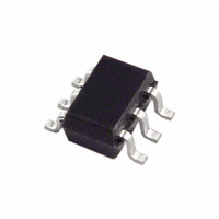
AD5612YKSZ-2REEL7 Analog Devices Inc, AD5612YKSZ-2REEL7 Datasheet - Page 15

AD5612YKSZ-2REEL7
Manufacturer Part Number
AD5612YKSZ-2REEL7
Description
IC,D/A CONVERTER,SINGLE,10-BIT,CMOS,TSSOP,6PIN
Manufacturer
Analog Devices Inc
Series
nanoDAC™r
Datasheet
1.AD5622AKSZ-2REEL7.pdf
(24 pages)
Specifications of AD5612YKSZ-2REEL7
Settling Time
6µs
Number Of Bits
10
Data Interface
I²C, Serial
Number Of Converters
1
Voltage Supply Source
Single Supply
Power Dissipation (max)
500µW
Operating Temperature
-40°C ~ 125°C
Mounting Type
Surface Mount
Package / Case
SC-70-6, SC-88, SOT-363
Lead Free Status / RoHS Status
Lead free / RoHS Compliant
THEORY OF OPERATION
D/A SECTION
The AD5602/AD5612/AD5622 DACs are fabricated on a
CMOS process. The architecture consists of a string DACs
followed by an output buffer amplifier. Figure 36 shows a block
diagram of the DAC architecture.
Since the input coding to the DAC is straight binary, the ideal
output voltage is given by
where:
D is the decimal equivalent of the binary code that is loaded
to the DAC register; it can range from 0 to 255 (AD5602),
0 to 1023 (AD5612), or 0 to 4095 (AD5622).
n is the bit resolution of the DAC.
RESISTOR STRING
The resistor string structure is shown in Figure 37. It is simply a
string of resistors, each of value R. The code loaded to the DAC
register determines at which node on the string the voltage is
tapped off to be fed into the output amplifier. The voltage is
tapped off by closing one of the switches connecting the string
to the amplifier. Because it is a string of resistors, it is
guaranteed monotonic.
DAC REGISTER
V
OUT
=
V
DD
×
⎛
⎜
⎝
Figure 36. DAC Architecture
2
D
n
⎞
⎟
⎠
NETWORK
RESISTOR
REF (+)
REF (–)
GND
V
DD
AMPLIFIER
OUTPUT
V
OUT
Rev. B | Page 15 of 24
OUTPUT AMPLIFIER
The output buffer amplifier is capable of generating rail-to-rail
voltages on its output, giving an output range of 0 V to V
capable of driving a load of 2 kΩ in parallel with 1000 pF to
GND. The source and sink capabilities of the output amplifier
can be seen in Figure 26. The slew rate is 0.5 V/μs with a half-
scale settling time of 5 μs with the output unloaded.
R
R
R
R
R
Figure 37. Resistor String Structure
AD5602/AD5612/AD5622
TO OUTPUT
AMPLIFIER
DD
. It is


