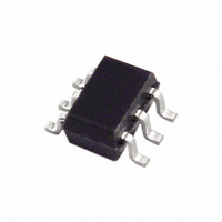
AD5612YKSZ-2REEL7 Analog Devices Inc, AD5612YKSZ-2REEL7 Datasheet

AD5612YKSZ-2REEL7
Specifications of AD5612YKSZ-2REEL7
Related parts for AD5612YKSZ-2REEL7
AD5612YKSZ-2REEL7 Summary of contents
Page 1
FEATURES Single 8-, 10-, 12-bit DACs, 2 LSB INL 6-lead SC70 package Micropower operation: 100 μA max @ 5 V Power-down to <150 2 5.5 V power supply Guaranteed monotonic by design Power-on reset ...
Page 2
AD5602/AD5612/AD5622 TABLE OF CONTENTS Features .............................................................................................. 1 Applications....................................................................................... 1 Functional Block Diagram .............................................................. 1 General Description ......................................................................... 1 Product Highlights ........................................................................... 1 Revision History ............................................................................... 2 Specifications..................................................................................... Timing Specifications............................................................ 4 Timing Diagram ........................................................................... 5 Absolute Maximum ...
Page 3
SPECIFICATIONS kΩ to GND Table 2. Parameter STATIC PERFORMANCE Resolution AD5602 AD5612 AD5622 2 Relative Accuracy AD5602 AD5612 AD5622 2 Differential Nonlinearity Zero Code Error Offset Error ...
Page 4
AD5602/AD5612/AD5622 Parameter POWER REQUIREMENTS (Normal Mode (All Power-Down Modes 4 5 ...
Page 5
Parameter Conditions t Standard mode 8 Fast mode High speed mode t Standard mode 9 Fast mode High speed mode 100 pF B High speed mode 400 Standard mode 10 Fast mode ...
Page 6
AD5602/AD5612/AD5622 ABSOLUTE MAXIMUM RATINGS T = 25°C, unless otherwise noted. A Table 4. Parameter V to GND DD Digital Input Voltage to GND V to GND OUT Operating Temperature Range Extended Automotive (W, Y Versions) Extended Industrial (A, B Versions) ...
Page 7
PIN CONFIGURATION AND FUNCTION DESCRIPTIONS Table 5. Pin Function Descriptions Pin No. Mnemonic Description 1 ADDR Three-State Address Input. Sets the two least significant bits (Bit A1, Bit A0) of the 7-bit slave address (see Table 6). 2 SCL Serial ...
Page 8
AD5602/AD5612/AD5622 TYPICAL PERFORMANCE CHARACTERISTICS 1 0 25°C A 0.6 0.4 0.2 0 –0.2 –0.4 –0.6 –0.8 –1.0 0 500 1000 1500 2000 2500 DAC CODE Figure 4. Typical AD5622 Integral Nonlinearity Error 0.15 V ...
Page 9
25° –1 –2 –3 –4 –5 –6 –7 0 500 1000 1500 2000 2500 3000 DAC CODE Figure 10. Typical AD5622 Total Unadjusted Error 0 25°C A MAX INL ...
Page 10
AD5602/AD5612/AD5622 0.6 0.5 0.4 MAX DNL = 5V 0.3 0.2 MAX DNL = 3V 0.1 0 MIN DNL = 5V –0.1 –0.2 MIN DNL = 3V –0.3 –40 – TEMPERATURE (°C) Figure 16. AD5622 DNL Error ...
Page 11
0.06 0. 0.04 0.03 0.02 0.01 0 –40 – TEMPERATURE (°C) Figure 22. Supply Current vs. Temperature (3 V/5 V Supply ...
Page 12
AD5602/AD5612/AD5622 CH1 CH2 CH1 = 5V/DIV, CH2 = 1V/DIV, TIME BASE = 2µs/DIV Figure 28. Exiting Power-Down Mode CH1 CH2 CH1 = 5V/DIV, CH2 = 1V/DIV, TIME BASE = 2µs/DIV Figure 29. Full-Scale Settling Time CH1 CH2 CH1 = 5V/DIV, ...
Page 13
25°C A MIDSCALE LOADED CH1 CH1 = 5µV/DIV Figure 34. 1/f Noise, 0 Bandwidth AD5602/AD5612/AD5622 700 25°C A 600 UNLOADED OUTPUT 500 400 ZERO ...
Page 14
AD5602/AD5612/AD5622 TERMINOLOGY Relative Accuracy For the DAC, relative accuracy or integral nonlinearity (INL measure of the maximum deviation, in LSBs, from a straight line passing through the endpoints of the DAC transfer function. A typical INL vs. code ...
Page 15
THEORY OF OPERATION D/A SECTION The AD5602/AD5612/AD5622 DACs are fabricated on a CMOS process. The architecture consists of a string DACs followed by an output buffer amplifier. Figure 36 shows a block diagram of the DAC architecture REF ...
Page 16
AD5602/AD5612/AD5622 SERIAL INTERFACE The AD5602/AD5612/AD5622 have 2-wire I 2 serial interfaces (refer to I C-Bus Specification, Version 2.1, January 2000, available from Philips Semiconductor). The AD5602/AD5612/AD5622 can be connected slave device, under the control of a master ...
Page 17
POWER-ON RESET The AD5602/AD5612/AD5622 each contain a power-on reset circuit that controls the output voltage during power-up. The DAC register is filled with zeros and the output voltage where it remains until a valid write sequence is ...
Page 18
AD5602/AD5612/AD5622 WRITE OPERATION When writing to the AD5602/AD5612/AD5622, the user must begin with a start command followed by an address byte ( 0), after which the DAC acknowledges that it is prepared to receive data by pulling SDA ...
Page 19
READ OPERATION When reading data back from the AD5602/AD5612/AD5622, the user begins with a start command followed by an address byte ( 1), after which the DAC acknowledges that SCL SDA START ...
Page 20
AD5602/AD5612/AD5622 HIGH SPEED MODE High speed mode communication commences after the master addresses all devices connected to the bus with the Master Code 00001XXX to indicate that a high speed mode transfer is to begin. No device connected to the ...
Page 21
APPLICATIONS CHOOSING A REFERENCE AS POWER SUPPLY The AD5602/AD5612/AD5622 come in tiny SC70 packages with less than 100 μA supply current, thereby making the choice of reference dependent upon the application requirement. For space-saving applications, the ADR425 is available in ...
Page 22
AD5602/AD5612/AD5622 OUTLINE DIMENSIONS 2.20 2.00 1.80 2.40 1. 1.25 2.10 1.80 1. PIN 1 0.65 BSC 1.30 BSC 1.00 0.40 1.10 0.90 0.10 0.80 0.70 0.30 0.10 MAX SEATING 0.15 PLANE 0.10 COPLANARITY COMPLIANT ...
Page 23
... LSB 1 AD5612YKSZ-1REEL7 ±0.5 LSB 1 AD5612BKSZ-2500RL7 ±0.5 LSB 1 AD5612BKSZ-2REEL7 ±0.5 LSB 1 AD5612AKSZ-2500RL7 ±4 LSB 1 AD5612AKSZ-2REEL7 ±4 LSB AD5612YKSZ-2500RL7 1 ±0.5 LSB 1 AD5612YKSZ-2REEL7 ±0.5 LSB 1 AD5622YKSZ-1500RL7 ±2 LSB 1 AD5622YKSZ-1REEL7 ±2 LSB 1 AD5622BKSZ-2500RL7 ±2 LSB 1 AD5622BKSZ-2REEL7 ±2 LSB AD5622YKSZ-2500RL7 1 ±2 LSB 1 AD5622YKSZ-2REEL7 ±2 LSB ...
Page 24
AD5602/AD5612/AD5622 NOTES 2 Purchase of licensed I C components of Analog Devices or one of its sublicensed Associated Companies conveys a license for the purchaser under the Philips I 2 Rights to use these components system, ...


