CYIS1SM1000-EVAL Cypress Semiconductor Corp, CYIS1SM1000-EVAL Datasheet - Page 5
CYIS1SM1000-EVAL
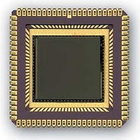
Manufacturer Part Number
CYIS1SM1000-EVAL
Description
MCU, MPU & DSP Development Tools 1M Pixel Radiation Hard CMOS Img Snsr
Manufacturer
Cypress Semiconductor Corp
Datasheet
1.CYIS1SM1000-EVAL.pdf
(24 pages)
Specifications of CYIS1SM1000-EVAL
Lead Free Status / RoHS Status
Lead free / RoHS Compliant


The pixel array contains 1024 by 1024 active pixels at 15µm pitch. Each pixel
contains one photo diode and three transistors (Figure 2).
The photo diode is always in reverse bias. At the beginning of the integration cycle a
pulse is applied to the reset line (gate of T1) bringing the cathode of D1 to the reset
voltage level. During the integration period photon-generated electrons accumulate
on the diode capacitance, reducing the voltage on the gate of T2.
illumination-dependent signal is the different between the reset level and the output
level after integration. This difference is made in the column amplifiers. T2 acts as a
source follower and T3 allows connection of the pixel signal (reset level and output
level) to the vertical output bus.
The reset-lines and the read-lines of the pixels in a row are connected together to the
Y-decoder logic; the outputs of the pixels in a column are connected together to a
column amplifier.
The addressing logic allows direct addressing of rows and columns. Instead of the
one-hot shift registers that are often used, address decoders are implemented. One
can select a line by presenting the required address to the address input of the device
and latching it to the Y-decoder logic. Presenting the X-address to the device address
input and latching it to the X-address decoder can select a column.
A typical line read out sequence will first select a line by applying the Y-address to
the Y-decoder. Activation of the “LD_Y” input on the Y-logic will connect the pixel
outputs of the selected line to the column amplifiers. The individual column amplifier
outputs can be connected to the output amplifier by applying the respective X-
addresses to the X address decoder. Applying the appropriate Y-address to the Y-
decoder and activating the “Reset” input reset a line. The integration time of a row is
the time between the last reset of this row and time when it is selected for read-out.
Cypress Semiconductor Corporation 3901 North First Street
Contact:
1.1.
1.2.
STAR-1000
Datasheet
info@Fillfactory.com
The pixel array
Addressing logic
Figure 2: Active pixel electrical diagram
Reset
Document #:38-05714 Rev.**(Revision 6.5)
T1
T2
Read
T3
San Jose, CA 95134 408-943-2600
Page 5 of 24
The real
Related parts for CYIS1SM1000-EVAL
Image
Part Number
Description
Manufacturer
Datasheet
Request
R

Part Number:
Description:
Manufacturer:
Cypress Semiconductor Corp
Datasheet:
Part Number:
Description:
Manufacturer:
Cypress Semiconductor Corp
Datasheet:
Part Number:
Description:
Manufacturer:
Cypress Semiconductor Corp
Datasheet:
Part Number:
Description:
Manufacturer:
Cypress Semiconductor Corp
Datasheet:
Part Number:
Description:
Manufacturer:
Cypress Semiconductor Corp
Datasheet: