MC33696MOD434EV Freescale Semiconductor, MC33696MOD434EV Datasheet - Page 7
MC33696MOD434EV
Manufacturer Part Number
MC33696MOD434EV
Description
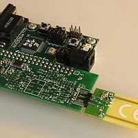
MCU, MPU & DSP Development Tools MC33696 (ECHO) RF C EVAL
Manufacturer
Freescale Semiconductor
Specifications of MC33696MOD434EV
Processor To Be Evaluated
MC9S08RG60
Interface Type
RS-232
Lead Free Status / RoHS Status
Lead free / RoHS Compliant


7
The receiver is based on a superheterodyne architecture with an intermediate frequency IF (see
Its input is connected to the RFIN pin. Frequency down conversion is done by a high-side injection I/Q
mixer driven by the frequency synthesizer. An integrated poly-phase filter performs rejection of the image
frequency.
The low intermediate frequency allows integration of the IF filter providing the selectivity. The IF Filter
center frequency is tuned by automatic frequency control (AFC) referenced to the crystal oscillator
frequency.
Sensitivity is met by an overall amplification of approximately 96 dB, distributed over the reception chain,
comprising low-noise amplifier (LNA), mixer, post-mixer amplifier, and IF amplifier. Automatic gain
control (AGC), on the LNA and the IF amplifier, maintains linearity and prevents internal saturation.
Sensitivity can be reduced using four programmable steps on the LNA gain.
Amplitude demodulation is achieved by peak detection. Frequency demodulation is achieved in two steps:
the IF amplifier AGC is disabled and acts as an amplitude limiter; a filter performs a frequency-to-voltage
conversion. The resulting signal is then amplitude demodulated in the same way as in the case of amplitude
modulation with an adaptive voltage reference.
A low-pass filter improves the signal-to-noise ratio of demodulated data. A data slicer compares
demodulated data with a fixed or adaptive voltage reference and provides digital level data.
This digital data is available if the integrated data manager is not used.
If used, the data manager performs clock recovery and decoding of Manchester coded data. Data and clock
are then available on the serial peripheral interface (SPI). The configuration sets the data rate range
managed by the data manager and the bandwidth of the low-pass filter.
An internal low-frequency oscillator can be used as a strobe oscillator to perform an automatic wakeup
sequence.
It is also possible to define two different configurations for the receiver (frequency, data rate, data manager,
modulation, etc.) that are automatically loaded during wakeup or under MCU control.
If the PLL goes out of lock, received data is ignored.
Freescale Semiconductor
Receiver Functional Description
If LVDE = 1, the LVD module remains enabled. The circuit cannot be put
in standby mode, but remains in LVD mode with a higher quiescent current,
due to the monitoring circuitry. LVD function is not accurate in standby
mode.
MC33696 Data Sheet, Rev. 12
NOTE
Receiver Functional Description
Figure
1).
7
Related parts for MC33696MOD434EV
Image
Part Number
Description
Manufacturer
Datasheet
Request
R

Part Number:
Description:
Manufacturer:
Freescale Semiconductor, Inc
Datasheet:
Part Number:
Description:
Manufacturer:
Freescale Semiconductor, Inc
Datasheet:
Part Number:
Description:
Manufacturer:
Freescale Semiconductor, Inc
Datasheet:
Part Number:
Description:
Manufacturer:
Freescale Semiconductor, Inc
Datasheet:
Part Number:
Description:
Manufacturer:
Freescale Semiconductor, Inc
Datasheet:
Part Number:
Description:
Manufacturer:
Freescale Semiconductor, Inc
Datasheet:
Part Number:
Description:
Manufacturer:
Freescale Semiconductor, Inc
Datasheet:
Part Number:
Description:
Manufacturer:
Freescale Semiconductor, Inc
Datasheet:
Part Number:
Description:
Manufacturer:
Freescale Semiconductor, Inc
Datasheet:
Part Number:
Description:
Manufacturer:
Freescale Semiconductor, Inc
Datasheet:
Part Number:
Description:
Manufacturer:
Freescale Semiconductor, Inc
Datasheet:
Part Number:
Description:
Manufacturer:
Freescale Semiconductor, Inc
Datasheet:
Part Number:
Description:
Manufacturer:
Freescale Semiconductor, Inc
Datasheet:
Part Number:
Description:
Manufacturer:
Freescale Semiconductor, Inc
Datasheet:
Part Number:
Description:
Manufacturer:
Freescale Semiconductor, Inc
Datasheet: