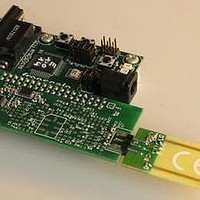
MC33696MOD434EV Freescale Semiconductor, MC33696MOD434EV Datasheet - Page 45

MC33696MOD434EV
Manufacturer Part Number
MC33696MOD434EV
Description
MCU, MPU & DSP Development Tools MC33696 (ECHO) RF C EVAL
Manufacturer
Freescale Semiconductor
Specifications of MC33696MOD434EV
Processor To Be Evaluated
MC9S08RG60
Interface Type
RS-232
Lead Free Status / RoHS Status
Lead free / RoHS Compliant
HD[5:0] (Header) sets the header. The header is Manchester coded. Its LSB corresponds to the register’s
LSB, whatever the specified length.
18.6 RSSI Register
Figure 34
Bits RSSI[7:4] contain the result of the analog-to-digital conversion of the signal measured at the LNA
output.
Bits RSSI[3:0] contain the result of the analog-to-digital conversion of the signal measured at the IF filter
output.
19
Registers are physically mapped following a byte organization. The possible address space is 32 bytes. The
base address is specified in the command byte. This is then incremented internally to address each register,
up to the number of registers specified by N[1:0], also specified by this command byte. All registers can
then be scanned, whatever the type of transmission (read or write); however, writing to read-only bits or
registers has no effect. When the last implemented address is reached, the internal address counter
automatically loops back to the first mapped address ($00).
At any time, it is possible to write or read the content of any register of Bank A and Bank B. Register access
is defined as follows:
Freescale Semiconductor
Reset Value
Bit Name
Access
R/W
R
RR
R [A]
RR [A]
Bank Access and Register Mapping
describes the RSSI Result register, RSSI.
RSSI7
Bit 7
R
0
Bit can be read and written.
Bit can be read. Write has no effect on bit value.
Bit can be read. Read or write resets the value.
Bit can be read. This returns the same value as Bank A.
Bit can be read. This returns the same value as Bank A. Read or write resets the value.
RSSI6
Bit 6
R
0
HDL1
0
0
1
1
Table 22. Header Length Selection
RSSI5
Bit 5
R
0
MC33696 Data Sheet, Rev. 12
Figure 34. RSSI Register
HDL0
0
1
0
1
RSSI4
Bit 4
R
0
RSSI3
Bit 3
R
0
HD Length
1 bits
2 bits
4 bits
6 bits
RSSI2
Bit 2
R
0
Bank Access and Register Mapping
RSSI1
Bit 1
R
0
RSSI0
Bit 0
R
0
Addr
$0C
45


