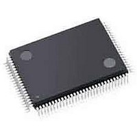
NJU6624CFG1-02 NJR, NJU6624CFG1-02 Datasheet - Page 28

NJU6624CFG1-02
Manufacturer Part Number
NJU6624CFG1-02
Description
LCD Drivers 14-Char/1-Line Dot Mtrx LCD Cntrlr Drvr
Manufacturer
NJR
Datasheet
1.NJU6624CFG1-02.pdf
(36 pages)
Specifications of NJU6624CFG1-02
Number Of Digits
14
Number Of Segments
70
Maximum Clock Frequency
218 KHz
Operating Supply Voltage
2.4 V to 5.5 V
Maximum Power Dissipation
500 mW
Maximum Operating Temperature
+ 85 C
Package / Case
QFP-100-G1
Maximum Supply Current
500 uA
Minimum Operating Temperature
- 40 C
Lead Free Status / RoHS Status
Lead free / RoHS Compliant
Available stocks
Company
Part Number
Manufacturer
Quantity
Price
Part Number:
NJU6624CFG1-02
Manufacturer:
JRC
Quantity:
20 000
(6)Interface with MPU
(6)Interface with MPU
The instructions and data are communicated with the serial port which is a clock synchronization type based on
The instructions and data are communicated with the serial port which is a clock synchronization type based on
16-bit per word.
16-bit per word.
The NJU6624A/B can be controlled by the serial data as shown below.
The NJU6624A/B can be controlled by the serial data as shown below.
CS
CS
SCL
SCL
DATA
DATA
The serial interface circuit operates in CS=L.
The serial interface circuit operates in CS=L.
A communication unit consists of 16-bit data. The communication period is from the falling edge of CS terminal to
A communication unit consists of 16-bit data. The communication period is from the falling edge of CS terminal to
the rising edge. The inputs data and latched at rising edge of shift clock (SCL) and the first 16-bit data are fetched
the rising edge. The inputs data and latched at rising edge of shift clock (SCL) and the first 16-bit data are fetched
into the NJU6624A/B at the rising edge of chip select (CS). The data over than 16 bits are ignored. If the input
into the NJU6624A/B at the rising edge of chip select (CS). The data over than 16 bits are ignored. If the input
data are less than 16 bits,they are ignored at the rising edge of "CS". Therefore,just 16 bits data should be input
data are less than 16 bits,they are ignored at the rising edge of "CS". Therefore,just 16 bits data should be input
for the correct communication. In case of RAM data input, the RAM address is changed automatically
for the correct communication. In case of RAM data input, the RAM address is changed automatically
as increment or decrement.
as increment or decrement.
The data to input is MSB first. Although the output data is just only key scan, data bits D8 to D15 in the key data
The data to input is MSB first. Although the output data is just only key scan, data bits D8 to D15 in the key data
read out instruction are input. After these 8-bit instruction is input, this serial data input terminal is changed to the
read out instruction are input. After these 8-bit instruction is input, this serial data input terminal is changed to the
output terminal at the 8th falling edge of SCL clock.
output terminal at the 8th falling edge of SCL clock.
The electrical short between the NJU6624A/B and external circuit must be prevented in the application.
The electrical short between the NJU6624A/B and external circuit must be prevented in the application.
NJU6624A/B
NJU6624A/B


