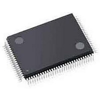
NJU6624CFG1-02 NJR, NJU6624CFG1-02 Datasheet - Page 15

NJU6624CFG1-02
Manufacturer Part Number
NJU6624CFG1-02
Description
LCD Drivers 14-Char/1-Line Dot Mtrx LCD Cntrlr Drvr
Manufacturer
NJR
Datasheet
1.NJU6624CFG1-02.pdf
(36 pages)
Specifications of NJU6624CFG1-02
Number Of Digits
14
Number Of Segments
70
Maximum Clock Frequency
218 KHz
Operating Supply Voltage
2.4 V to 5.5 V
Maximum Power Dissipation
500 mW
Maximum Operating Temperature
+ 85 C
Package / Case
QFP-100-G1
Maximum Supply Current
500 uA
Minimum Operating Temperature
- 40 C
Lead Free Status / RoHS Status
Lead free / RoHS Compliant
Available stocks
Company
Part Number
Manufacturer
Quantity
Price
Part Number:
NJU6624CFG1-02
Manufacturer:
JRC
Quantity:
20 000
(4)Instructions
(4)Instructions
The NJU6624A/B incorporates two registers, an Instruction Register (IR) and a Data Register(DR).
The NJU6624A/B incorporates two registers, an Instruction Register (IR) and a Data Register(DR).
These two registers store control information temporarily to allow interface between NJU6624A/B and MPU or
These two registers store control information temporarily to allow interface between NJU6624A/B and MPU or
peripheral ICs operating different cycles.
peripheral ICs operating different cycles.
MS1,MS0 : Discriminate master or slave. And write code (meet code for selected device) like as mentioned
MS1,MS0 : Discriminate master or slave. And write code (meet code for selected device) like as mentioned
Note : f
Note : f
(m) Set CG RAM
(a) Maker Testing
(b) Clear Display
(c) Return Home
(d) Entry Mode Set
(e) Display ON/OFF
(g) Display Shift
(h) Set Static Port
(k)
(n)
(o) Read Keyscan
(f) Address Shift
(i) Contrast Control
(j) Dot Shift
(l) Set DD/MK RAM
INSTRUCTION
Write DD RAM
Write MK RAM
Write CG RAM
Set Display
OSC
OSC
=145KHz. If the oscillation frequency is changed, the execution time is also changed.
=145KHz. If the oscillation frequency is changed, the execution time is also changed.
below.
below.
Address
Address
Control
Mode
Data
Data
Data
Data
D15 D14 D13 D12
MS1 MS0
MS1 MS0
MS1 MS0
MS1 MS0
MS1 MS0
MS1 MS0
MS1 MS0
MS1 MS0
MS1 MS0
MS1 MS0
MS1 MS0
MS1 MS0
MS1 MS0
MS1 MS0
MS1 MS0
MS1 MS0
MS1 MS0
MS1
0
1
0
0
0
0
0
0
0
0
0
0
0
0
0
0
0
0
1
MS0
0
0
0
0
0
0
0
0
1
1
1
1
1
1
1
1
1
0
1
Table 4. Table of Instructions
Table 4. Table of Instructions
D11 D10
0
0
0
0
0
1
1
1
1
1
1
1
1
1
1
1
1
NJU6624A
NJU6624B
0
0
0
0
0
0
0
0
0
0
0
0
1
1
1
1
1
D9 D8 D7 D6 D5 D4 D3 D2 D1 D0
0
0
0
0
0
0
0
0
0
0
1
1
1
1
1
1
1
DEVICE
CODE
0
0
0
0
0
0
0
0
0
1
1
1
1
1
1
1
1
*
*
*
*
*
*
*
*
*
*
*
*
*
*
*
*
*
*
*
*
*
*
*
*
*
*
Write data(DD RAM)
CG RAM(00 to FE)H
*
*
*
*
*
*
*
*
*
*
*
*
*
Test data
Key Data
DD RAM(00 to 0D)H
Write data(MK RAM)
*
*
*
*
*
*
*
*
*
*
MK RAM(10 to 1B)H
Write data(CGRAM)
P3 P2 P1 P0
*
*
*
*
*
*
*
*
E.V.R. Value
Number of
NJU6624A/B
NJU6624A/B
D
*
*
*
*
*
*
Dot Shift
I/D
M
K
*
*
*
*
DRL
ARL
PD
S
B
*
*
234.48uS
41.38uS
41.38uS
41.38uS
Execute
Time
0uS
0uS
0uS
0uS
0uS
0uS
0uS
0uS
0uS
0uS
0uS
0uS
-


