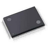
NJU6624CFG1-02 NJR, NJU6624CFG1-02 Datasheet - Page 25

NJU6624CFG1-02
Manufacturer Part Number
NJU6624CFG1-02
Description
LCD Drivers 14-Char/1-Line Dot Mtrx LCD Cntrlr Drvr
Manufacturer
NJR
Datasheet
1.NJU6624CFG1-02.pdf
(36 pages)
Specifications of NJU6624CFG1-02
Number Of Digits
14
Number Of Segments
70
Maximum Clock Frequency
218 KHz
Operating Supply Voltage
2.4 V to 5.5 V
Maximum Power Dissipation
500 mW
Maximum Operating Temperature
+ 85 C
Package / Case
QFP-100-G1
Maximum Supply Current
500 uA
Minimum Operating Temperature
- 40 C
Lead Free Status / RoHS Status
Lead free / RoHS Compliant
Available stocks
Company
Part Number
Manufacturer
Quantity
Price
Part Number:
NJU6624CFG1-02
Manufacturer:
JRC
Quantity:
20 000
(n)Write Data to CG, DD or MK RAM
(n)Write Data to CG, DD or MK RAM
(o)Read Data Key
(o)Read Data Key
By the execution of this instruction, the binary 8-bit data (A
By the execution of this instruction, the binary 8-bit data (A
bit data (A
bit data (A
struction. After this instruction execution, the address increment (+1) or decrement(-1) is performed automatically
struction. After this instruction execution, the address increment (+1) or decrement(-1) is performed automatically
according to the entry mode set. And the display shift is also executed according to the previous entry mode set.
according to the entry mode set. And the display shift is also executed according to the previous entry mode set.
However, the data in MK RAM (1C)H and (1D)H are not displayed, bat the automatic address increment is per-
However, the data in MK RAM (1C)H and (1D)H are not displayed, bat the automatic address increment is per-
formed. And the display is not changed by the data written into MK RAM (1C)H and (1D)H
formed. And the display is not changed by the data written into MK RAM (1C)H and (1D)H
Read data key is a instruction for data reading out of keyscan. However, the bit 8 to 15 are input data. After this 8-
Read data key is a instruction for data reading out of keyscan. However, the bit 8 to 15 are input data. After this 8-
bit data were input, the operation change to output from input at the falling edge of 8th SCK clock.
bit data were input, the operation change to output from input at the falling edge of 8th SCK clock.
-Write Data to DD RAM
-Write Data to DD RAM
-Write Data to MK RAM
-Write Data to MK RAM
-Write Data to CG RAM
-Write Data to CG RAM
4 4
to A
to A
Code
Code
Code
Code
0 0
) are written into the CG or MK RAM. The selection of RAM is determined by the previous in-
) are written into the CG or MK RAM. The selection of RAM is determined by the previous in-
D15 D14 D13 D12 D11 D10 D9
D15 D14 D13 D12 D11 D10 D9
D15 D14 D13 D12 D11 D10 D9
D15 D14 D13 D12 D11 D10 D9
MS1 MS0
MS1 MS0
MS1 MS0
MS1 MS0
0
0
0
1
0
1
1
1
0
0
0
1
0
0
0
1
0
0
0
1
7 7
to A
to A
D8
D8
D8
D8
0
0
0
1
0 0
) are written into the DD RAM, and the binary 5-
) are written into the DD RAM, and the binary 5-
DD7 DD6 DD5 DD4 DD3 DD2 DD1 DD0
KL3 KL2 KL1 KL0
D7
D7
D7
D7
*
*
D6
D6
D6
D6
*
*
D5
D5
D5
D5
*
*
NJU6624A/B
NJU6624A/B
DM4 DM3 DM2 DM1 DM0
DC4 DC3 DC2 DC1 DC0
D4
D4
D4
D4
D3
D3
D3
D3
0
KH2 KH1 KH0
D2
D2
D2
D2
D1
D1
D1
D1
D0
D0
D0
D0


