LS013B4DN01 Sharp Microelectronics, LS013B4DN01 Datasheet - Page 11
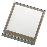
LS013B4DN01
Manufacturer Part Number
LS013B4DN01
Description
LCD Graphic Display Modules & Accessories 1.35 96x96 w/o FPC Mono Memory LCD
Manufacturer
Sharp Microelectronics
Datasheet
1.LS013B4DN01.pdf
(29 pages)
Specifications of LS013B4DN01
Pixel Density
96 x 96
Module Size (w X H X T)
28.2 mm x 32.34 mm x 1.4 mm
Viewing Area (w X H)
24.192 mm x 24.192 mm
Operating Temperature Range
- 20 C to + 70 C
Attached Touch Screen
No
Display Mode
Color - TFT
Product
TFT-LCD Module
Lead Free Status / RoHS Status
Lead free / RoHS Compliant


6-2)Power supply sequence
[Remark] Precaustions at ehte time of power on and power off.
VDD/VDDA (5V)
DISP
EXTCOMIN
SCS
Others
[On sequence] * All on start up System
① 5V start up
② Initializes memory data within pixel
Initialize with D2 "all clear flag" or display all white.
③ To cancel latch initialization for TCOM.
④ TCOM polarity initialization
The period of initialization for TCOM polarity by EXTCOMIN signal.
[Normal operation]
Duration of normal driving.
[Off sequence]
⑤ Initializes memory data within pixel
⑥ The period of initialization for VA, VB, and VCOM
⑦ 5V shut down
※ Detail description for signal timing is shown the digital timing chart and the AC timing chart.
※ 1 The order of ③ and ④ can be set as being reversed, in this case, TCOM polarity inversion timing which can be controlled
by EXTCOMIN doesn't work during DISP="L".
※ 2 Setup value for initialization of data within pixel memory
The period of canceling COM latch circuit for initialization by using DISP signal.
To refer the timing chart of all clear mode section 6-5-4.
Remark 1)When power on , VDDand VDDA are same timem or VDD should be faster than the VDDA.
Remark 2) When power off, VDD and VDDA are same time or VDDA shoud be faster than the VDD.
GND
GND
GND
GND
GND
①
T1
※ 2
※ 2
On Sequence
②
T2
③※ 1 ④※ 1
T3
T4
SPEC No.
LCY-12T09302A
Normal operation
Normal operation
Normal operation
Normal operation
T2 : more than 1V
T3 : more than 30us
T4: more than 30us
T5 : more than 1V
T6 : more than 1V
MODEL No.
※ 2
※ 2
⑤
T5
LS013B4DN01
Off Sequence
⑥
T6
⑦
T7
GND
GND
GND
GND
GND
PAGE
9
Related parts for LS013B4DN01
Image
Part Number
Description
Manufacturer
Datasheet
Request
R

Part Number:
Description:
IC FLASH 32MBIT 110NS 56SSOP
Manufacturer:
Sharp Microelectronics
Datasheet:

Part Number:
Description:
IC FLASH 16MBIT 100NS 56TSOP
Manufacturer:
Sharp Microelectronics
Datasheet:

Part Number:
Description:
IC FLASH 64MBIT 120NS 56TSOP
Manufacturer:
Sharp Microelectronics
Datasheet:

Part Number:
Description:
IC FLASH 16MBIT 90NS 48TSOP
Manufacturer:
Sharp Microelectronics
Datasheet:
Part Number:
Description:
IC SRAM 16KBIT 100NS 24DIP
Manufacturer:
Sharp Microelectronics
Datasheet:
Part Number:
Description:
IC SRAM 16KBIT 100NS 24SOP
Manufacturer:
Sharp Microelectronics
Datasheet:
Part Number:
Description:
IC SRAM 64KBIT 100NS 28DIP
Manufacturer:
Sharp Microelectronics
Datasheet:
Part Number:
Description:
IC SRAM 64KBIT 100NS 28SOP
Manufacturer:
Sharp Microelectronics
Datasheet:
Part Number:
Description:
IC SRAM 64KBIT 100NS 28SOP
Manufacturer:
Sharp Microelectronics
Datasheet:
Part Number:
Description:
IC SRAM 256KBIT 70NS 28DIP
Manufacturer:
Sharp Microelectronics
Datasheet:
Part Number:
Description:
IC FLASH 8MBIT 90NS 48TSOP
Manufacturer:
Sharp Microelectronics
Datasheet:
Part Number:
Description:
IC FLASH 8MBIT 85NS 40TSOP
Manufacturer:
Sharp Microelectronics
Datasheet:
Part Number:
Description:
IC FLASH 8MBIT 85NS 40TSOP
Manufacturer:
Sharp Microelectronics
Datasheet:
Part Number:
Description:
IC FLASH 16MBIT 90NS 48TSOP
Manufacturer:
Sharp Microelectronics
Datasheet:
Part Number:
Description:
IC FLASH 16MBIT 70NS 56TSOP
Manufacturer:
Sharp Microelectronics
Datasheet: