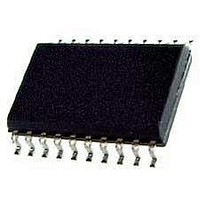
HV6810WG Supertex, HV6810WG Datasheet - Page 6

HV6810WG
Manufacturer Part Number
HV6810WG
Description
Display Drivers HVCMOS 10Chl Latched
Manufacturer
Supertex
Datasheet
1.HV6810PJ-G.pdf
(9 pages)
Specifications of HV6810WG
Driver Type
VFD Drivers
Operating Supply Voltage
7.5 V
Maximum Operating Temperature
+ 85 C
Mounting Style
SMD/SMT
Package / Case
SOIC-20 Wide
Minimum Operating Temperature
- 40 C
Supply Current
50 mA
Lead Free Status / RoHS Status
Lead free / RoHS Compliant
Available stocks
Company
Part Number
Manufacturer
Quantity
Price
Part Number:
HV6810WG
Manufacturer:
SUPERTE
Quantity:
20 000
Pin Descriptions
20-Lead PLCC (PJ)
Pin #
10
11
12
13
14
15
16
17
18
19
20
1
2
3
4
5
6
7
8
9
Supertex inc.
SERIAL DATA OUT
LE (STROBE)
BLANKING
Function
DATA IN
CLOCK
VDD
VSS
VBB
Q10
N/C
N/C
Q8
Q7
Q6
Q5
Q4
Q3
Q2
Q1
Q9
●
1235 Bordeaux Drive, Sunnyvale, CA 94089
Description
High voltage output.
Input data is shifted into the data shift register on the positive edge of the clock.
No connection.
Usually V
Low voltage power supply.
When LE is high, the shift register output is latched to Q output. When LE stays high,
the latches are in transparent mode.
High voltage output.
When blanking is high, all Q’s are forced to a low state, regardless of data in each
channel.
Input data for the input shift register.
No connection.
High voltage power supply.
Output data from the shift register.
High voltage output.
SS
= 0V, ground connection.
6
●
Tel: 408-222-8888
●
www.supertex.com
HV6810


