HV6810WG Supertex, HV6810WG Datasheet
HV6810WG
Specifications of HV6810WG
Available stocks


Related parts for HV6810WG


HV6810WG Summary of contents
Page 1
... Supertex inc. Features ► High output voltage 80V ► High speed 5MHz @5.0V DD ► Low power I ≤ 0.1mA (all high) BB ► Active pull down 100µA min @25 ► Output source current 25mA @60V V ► Each device drives 10 lines ► High-speed serially-shifted data input ► ...
Page 2
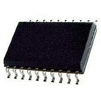
... Continuous high-level Q output current OH f Clock frequency CLK T Operating ambient temperature A Supertex inc. Pin Configuration 20-Lead SOW 12.80x7.50mm body 2.65mm height (max) 1.27mm pitch HV6810WG-G Product Marking 1 Value 7.5V 90V 90V -0. 0.3V DD Package may or may not include the following marks 1500mW 1500mW 1 -45° ...
Page 3
... SS 2. Apply Set all inputs (Data, CLK, Enable, etc known state 4. Apply V BB The V should not drop below V or float during operation Power-down sequence should be the reverse of the above. Supertex inc. Min Typ Q outputs 57.5 58 Serial output 4.0 4.5 Q outputs - 0.15 ...
Page 4
... W(CKH) 50% Clock t SU(D) Valid Data 50% 50% Input Timing Timing Diagram Clock Data In SR Contents Latch Enable Latch PREVIOUSLY STORED DATA Contents Blanking Q Outputs Supertex inc Clock 50% Input Latch H(D) Enable Output V IL VALID IRRELEVANT INVALID ● 1235 Bordeaux Drive, Sunnyvale, CA 94089 ...
Page 5
... Contents Input Input ... ... N ... N ... ... X --- --- ... --- Notes Low logic level High logic level Don’t care Present state Previous state = Low to high transition = High to low transition Supertex inc. Serial LE Latch Contents Data Strobe Output Input 1 N N-1 N --- N --- --- ... X ● 1235 Bordeaux Drive, Sunnyvale, CA 94089 ...
Page 6
... N/C 17 VBB 18 SERIAL DATA OUT 19 Q10 20 Q9 Supertex inc. Description High voltage output. Input data is shifted into the data shift register on the positive edge of the clock. No connection. Usually V = 0V, ground connection. SS Low voltage power supply. When LE is high, the shift register output is latched to Q output. When LE stays high, the latches are in transparent mode ...
Page 7
... VBB 17 SERIAL DATA OUT 18 N/C 19 Q10 20 Q9 Supertex inc. Description High voltage output. Input data are shifted into the data shift register on the positive edge of the clock. Usually V = 0V, ground connection connection. Low voltage power supply. When LE is high, the shift register output is latched to Q output. When LE stays high, the latches are in transparent mode ...
Page 8
... Actual shape of this feature may vary. Symbol A MIN .165 Dimension NOM .172 (inches) MAX .180 JEDEC Registration MS-018, Variation AA, Issue A, June, 1993. Drawings not to scale. Supertex Doc. #: DSPD-20PLCCPJ, Version B092408 Supertex inc Note 1 18 (Index Area Top View View B ...
Page 9
... JEDEC Registration MS-013, Variation AC, Issue E, Sep. 2005. * This dimension is not specified in the JEDEC drawing. Drawings are not to scale. Supertex Doc. #: DSPD-20SOWWG, Version D041309. (The package drawings in this data sheet may not reflect the most current specifications. For the latest package outline information go to http://www.supertex.com/packaging.html.) does not recommend the use of its products in life support applications, and will not knowingly sell them for use in such applications unless it receives Supertex inc ...