HFBR-0564 Avago Technologies US Inc., HFBR-0564 Datasheet - Page 2
HFBR-0564
Manufacturer Part Number
HFBR-0564
Description
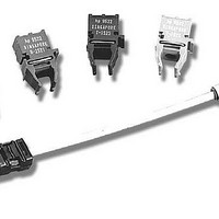
Fiber Optics, Evaluation Kit
Manufacturer
Avago Technologies US Inc.
Datasheet
1.HFBR-0562.pdf
(14 pages)
Specifications of HFBR-0564
Silicon Manufacturer
Avago
Silicon Core Number
HFBR-591xE
Kit Application Type
Communication & Networking
Application Sub Type
MT-RJ Gigabit Ethernet Transceiver
Main Purpose
Interface, Ethernet
Embedded
No
Utilized Ic / Part
HFCT-591xE, HFBR-591xE
Primary Attributes
MT-RJ Gigabit, Multimode and Singlemode Applications
Secondary Attributes
MT-RJ Fiber Connector Interface
Operating Voltage
3.3 V
Description/function
Fiber Optic Kit
Lead Free Status / RoHS Status
Lead free / RoHS Compliant
For Use With/related Products
HFBR-591x, HFCT-591
Lead Free Status / RoHS Status
Lead free / RoHS Compliant, Contains lead / RoHS non-compliant


2
The laser is designed to operate with
a 50% duty cycle or balanced signal,
for normal operation. Failure to
provide this may cause the optical
parameters to move out of speci-
fication. Extinction ratio and duty
cycle distortion may be affected. In
the absence of data the module will
emit a mean optical power within
the specified limit.
Optical Output
Figure
HFBR-591xE
waveform using the Gbe mask and
optical filter.
Figure
HFCT-591xE
waveform using the Gbe mask and
optical filter.
Power Supply Filtering
Good power supply filtering is
required for optimum transmitter per-
formance. The LC filtering technique
illustrated in the circuit diagram of
Figure 4 is recommended for the
user, when using separated trans-
mitter and receiver power supplies.
When using this filter arrangement,
supply noise greater than 100 mV
pk-pk, over a frequency range of
10 Hz to 1 MHz, can be tolerated
before the transmitter waveform
is compromised.
performance, the power supply
filter should be located as close as
possible to the supply pin of the
transceiver.
Transmitter Disable
In normal operation (transmit-
ter enabled), pin 8 should be left
open circuit. The transmitter can
be disabled by connecting pin 8 to
VCCT via a 500 W resistor. This input
pin requires a minimum of 50 µA for
it to operate.
1a
1b
transmitter
transmitter
shows
shows
For
a
a
optimum
output
output
typical
typical
Receiver
Supply Voltage
The transceiver modules require a
positive power supply in the range
of 3.14 V to 3.47 V. Care should be
taken to avoid supply transients
(see receiver ‘Power Supply Filtering’
section).
Figure 1a. Typical HFBR-591xE transmitter output showing Gbe mask at +25° C, +3.3 V
Figure 1b. Typical HFCT-591xE transmitter output showing Gbe mask at +25° C, +3.3 V
Power Supply Filtering
Good power supply filtering is
required for optimum receiver per-
formance. The LC filtering technique
illustrated in the circuit diagram of
Figure 4 is recommended. When
using this filter arrangement, supply
noise greater than 100 mV pk-pk,
over a frequency range of 10 Hz
to 1 MHz, can be tolerated before
a receiver sensitivity penalty of
1.0 dB occurs.
Related parts for HFBR-0564
Image
Part Number
Description
Manufacturer
Datasheet
Request
R

Part Number:
Description:
Fiber Optic Transmitters, Receivers, Transceivers 1300nm 155MBd 16-pin DIP ST Rx
Manufacturer:
Avago Technologies US Inc.

Part Number:
Description:
FIBER OPTIC TX 125 MBD 650N
Manufacturer:
Avago Technologies US Inc.
Datasheet:

Part Number:
Description:
Fiber Optic Evaluation Kit
Manufacturer:
Avago Technologies US Inc.
Datasheet:

Part Number:
Description:
RECEIVER FIBER OPTIC ST 266MBD
Manufacturer:
Avago Technologies US Inc.
Datasheet:

Part Number:
Description:
RCVR OPT HI SPEED VERS LINK HORZ
Manufacturer:
Avago Technologies US Inc.
Datasheet:

Part Number:
Description:
RCVR OPT HI SPEED VERS LINK VERT
Manufacturer:
Avago Technologies US Inc.
Datasheet:

Part Number:
Description:
TXRX OPTICAL 850NM VCSEL MT-RJ
Manufacturer:
Avago Technologies US Inc.
Datasheet:

Part Number:
Description:
TXRX MM SFP LC CONN BAIL DELATCH
Manufacturer:
Avago Technologies US Inc.
Datasheet:

Part Number:
Description:
TXRX MMF SFP GBE/FC BAIL DELATCH
Manufacturer:
Avago Technologies US Inc.
Datasheet:

Part Number:
Description:
XMITTER FIBER OPTIC 266MBD ST
Manufacturer:
Avago Technologies US Inc.
Datasheet:

Part Number:
Description:
OPTOCOUPLER GATE DRV 2A 16-SOIC
Manufacturer:
Avago Technologies US Inc.
Datasheet:
Part Number:
Description:
OPTOCOUPLER 2CH 2.5A 16-SOIC
Manufacturer:
Avago Technologies US Inc.
Datasheet:

Part Number:
Description:
OPTOCOUPLER GATE DRV 0.4A 16SOIC
Manufacturer:
Avago Technologies US Inc.
Datasheet:

Part Number:
Description:
OPTOCOUPLER 2.0A 250KHZ 8-DIP
Manufacturer:
Avago Technologies US Inc.
Datasheet:

Part Number:
Description:
OPTOCOUPLER 2.0A 250KHZ GW 8-SMD
Manufacturer:
Avago Technologies US Inc.
Datasheet: