HFBR-0564 Avago Technologies US Inc., HFBR-0564 Datasheet
HFBR-0564
Specifications of HFBR-0564


Related parts for HFBR-0564


HFBR-0564 Summary of contents
Page 1
... Small Form Factor (SFF) Gigabit Ethernet transceiver products. The HFCT-591xE is a single mode receptacled pinout transceiver. The HFBR-591xE is a multimode re- ceptacled pinout transceiver. Both are designed to be compliant with the IEEE Gigabit Ethernet 1000 Base-LX requirements. Figure 15 shows the pin assign- ment diagram and additional pinout information is provided in Table 1 ...
Page 2
... V to 3.47 V. Care should be taken to avoid supply transients (see receiver ‘Power Supply Filtering’ section). Figure 1a. Typical HFBR-591xE transmitter output showing Gbe mask at +25° C, +3.3 V Figure 1b. Typical HFCT-591xE transmitter output showing Gbe mask at +25° C, +3.3 V Power Supply Filtering Good power supply filtering is required for optimum receiver per- formance ...
Page 3
... It has a four layer FR-4 printed circuit board with ground planes on both sides designed to be footprint compatible for all single and multi - mode Gigabit Ethernet variants. 3 Figure 2a. Typical HFBR-591xE receiver output at +25° C, +3.3 V Figure 2b. Typical HFCT-591xE receiver output at +25° C, +3.3 V Figure 3. Test fixture ...
Page 4
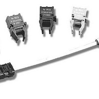
Edge-mounted SMA connectors are provided for data inputs and data outputs. Standard 2 mm sockets are included for easy connection to DC power supplies. A sliding switch is provided for selecting the transmitter disable function. Gold contact pin sockets are ...
Page 5
... HFBR/HFCT-591XE will operate in both configurations recommended bypass capacitor for additional low frequency noise filtering. The signal detect output on the HFBR-591XE contains an internal 1.8 k pull up resistor. The output stage on the HFCT-591XE pull configuration and therefore does not require an external pull up resistor. ...
Page 6
... Ground tabs must be connected to signal ground for optimum performance of the transceiver. The two front standoffs are metallized and at chassis ground. The two rear standoffs are at signal ground. Figure 6. HFBR-5912E 1.25 Gb multimode SFF Figure 7. HFCT-5912E 1.25 Gb/s single mode SFF ...
Page 7
... All dimensions on the circuit board layout and MT-RJ front panel layout were taken directly or indirectly from the joint MSA. Shown in Figure 8 is the recom- mended PCB layout for the HFBR/ HFCT-591xE. The distance from solder posts to front panel is critical in ensuring Ø 1.4 ±0.1 (0.055 ± ...
Page 8
... The 10 I/O pins, 2 solder posts and 4 package grounding tabs are to be treated as a single patter (See fFgure 5 PCB layout). 4. The MT-RJ has a 750 m fiber spacing. 5. The MT-RJ alignment pins are in the module. 6. See MT-RJ transceiver pin out diagram for details. Figure 9. Package outline drawing of HFBR/HFCT-591xE 8 13.97 (0.55) MIN. ...
Page 9
... In addition metals that can build up insulating oxides, such as aluminium, should be avoided. The SFF grounding scheme is de- scribed in the relevant data sheets important to note that the HFBR/HFCT-591xE transceivers have separate V planes but common CC ground planes for the transmitter and receiver sections. ...
Page 10
... EMI Radiation/Susceptibility Radiated emissions for the HFBR- 591xE and HFCT-591xE have been tested successfully in several en- vironments. Data sheet values will normally describe emissions be- havior in a worst-case, open air, un- shielded environment ...
Page 11
... Figure 11. HFBR-591xE open air radiation Figure 12. HFBR-591xE simulated chassis radiation Handling Process Plug The HFBR-591xE and HFCT-591xE SFF transceivers are supplied with a process plug for protection of optical ports. This process plug prevents contamination during solder and aqueous rinse as well as during handling, shipping or storage ...
Page 12
... Figure 14. HFCT-591xE simulated chassis radiation. Maximum emission below 960 MHz is 33.3 dBmV/m. Regulatory Notes Laser Safety – European Union The HFCT-591xE transceiver contains a 1300 nm FP laser. The HFBR-591xE transceiver contains a 850 nm VCSEL laser. These transceivers are classi- fied as “Class 1 Laser Products” per EN 60825-1(+A11), Safety of Laser Products ...
Page 13
RX Package Top Grounding Tabs View o RECEIVER SIGNAL GROUND 1 o RECEIVER POWER SUPPLY 2 o SIGNAL DETECT 3 o RECEIVER DATA OUT BAR 4 o RECEIVER DATA OUT 5 Figure 15. Pin assignment diagram Table 1. Pinout Table ...
Page 14
For product information and a complete list of distributors, please go to our web site: Avago, Avago Technologies, and the A logo are trademarks of Avago Technologies in the United States and other countries. Data subject to change. Copyright © ...