AD9858/PCBZ Analog Devices Inc, AD9858/PCBZ Datasheet - Page 5
AD9858/PCBZ
Manufacturer Part Number
AD9858/PCBZ
Description
DIGITAL SYNTHESIZER
Manufacturer
Analog Devices Inc
Specifications of AD9858/PCBZ
Silicon Manufacturer
Analog Devices
Application Sub Type
Direct Digital Synthesizer
Kit Application Type
Clock & Timing
Silicon Core Number
AD9858
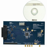
Kit Contents
Board
Design Resources
Low Jitter Sampling Clock Generator for High Performance ADCs Using AD9958/9858 and AD9515 (CN0109)
Main Purpose
Timing, Direct Digital Synthesis (DDS)
Utilized Ic / Part
AD9858/TL
Lead Free Status / RoHS Status
Lead free / RoHS Compliant
Embedded
-
Primary Attributes
-
Secondary Attributes
-
Lead Free Status / RoHS Status
Lead free / RoHS Compliant, Lead free / RoHS Compliant
Other names
AD9858/PCB
AD9858/PCB
AD9858/PCB


CONTROL WINDOW
The control window allows the user to set many of the
operating parameters of the device. In the Clock pane, the user
can specify the current clock frequency supplied to the device.
If the user desires, the clock divide-by-2 feature may be enabled.
After selecting this option, the user must click the LOAD
button. Until the LOAD button is clicked, it flashes green
indicating that a data change has been made but not loaded yet.
The clock divide-by-2 must be enabled for any clock frequency
exceeding 1 GHz.
To conserve power, the user may power down different
subsystems on the device, or perform a full power-down.
Under the Output Options pane, users may specify whether
they want a sine or cosine output. This is also where the user
enables frequency-sweeping mode, although the parameters for
the frequency sweep are edited in the profiles screen.
To the right are check boxes that control different bits to be set
or cleared in the control register. The auto clear frequency
accumulator and auto clear phase accumulator bits work as
follows. When set, upon receiving a FUD, the frequency and
Figure 8. Control Window
Rev. 0 | Page 5 of 12
phase accumulators are cleared. Then, the frequency and phase
accumulators begin accumulating at whatever rate is stored in
the delta frequency tuning word (frequency accumulator) and
the frequency tuning word (phase accumulator). When this bit
is not set, changes to the frequency and phase accumulators are
made in association with the values already stored there. The
load delta freq. timer specifies whether the device should wait
for a FUD signal before internally updating the value stored for
the delta frequency ramp rate word (box checked) or whether it
should automatically load new delta frequency ramp rate words
(box cleared). The clear frequency accumulator bit resets the
frequency accumulator and holds the value at zero until this bit
is cleared. The clear phase accumulator resets the phase
accumulator and holds the value at zero until the bit is cleared.
The SYNC clock Out disable pin causes the SYNC clock output
stage to be disabled and the pin to become high impedance. The
SYNC clock circuitry is still functioning internally, and the
SYNC clock signal can be re-enabled when this bit is cleared.
At the bottom of the screen are buttons that open the I/O
Interface window and the PLL Fast Lock window.
AD9858PCB
Related parts for AD9858/PCBZ
Image
Part Number
Description
Manufacturer
Datasheet
Request
R

Part Number:
Description:
BOARD EVAL TRANSLATION LOOP
Manufacturer:
Analog Devices Inc
Datasheet:
Part Number:
Description:
BOARD EVAL FOR AD9858/FD
Manufacturer:
Analog Devices Inc
Datasheet:
Part Number:
Description:
BOARD EVAL FOR AD9858/TL
Manufacturer:
Analog Devices Inc
Datasheet:

Part Number:
Description:
±1.7g Dual-Axis IMEMS Accelerometer Evaluation Board
Manufacturer:
Analog Devices Inc
Datasheet:
Part Number:
Description:
Inertial Sensor Evaluation System
Manufacturer:
Analog Devices Inc
Datasheet:
Part Number:
Description:
Manufacturer:
Analog Devices Inc
Datasheet:
Part Number:
Description:
Manufacturer:
Analog Devices Inc
Datasheet:
Part Number:
Description:
Manufacturer:
Analog Devices Inc
Datasheet:
Part Number:
Description:
Manufacturer:
Analog Devices Inc
Datasheet:
Part Number:
Description:
Manufacturer:
Analog Devices Inc
Datasheet:
Part Number:
Description:
Manufacturer:
Analog Devices Inc
Datasheet:
Part Number:
Description:
Manufacturer:
Analog Devices Inc
Datasheet:
Part Number:
Description:
Manufacturer:
Analog Devices Inc
Datasheet: