AD9858/PCBZ Analog Devices Inc, AD9858/PCBZ Datasheet

DIGITAL SYNTHESIZER

AD9858/PCBZ

Manufacturer Part Number
AD9858/PCBZ
Description
DIGITAL SYNTHESIZER
Manufacturer
Analog Devices Inc
Datasheets

Specifications of AD9858/PCBZ

Silicon Manufacturer
Analog Devices
Application Sub Type
Direct Digital Synthesizer
Kit Application Type
Clock & Timing
Silicon Core Number
AD9858
Kit Contents
Board
Design Resources
Low Jitter Sampling Clock Generator for High Performance ADCs Using AD9958/9858 and AD9515 (CN0109)
Main Purpose
Timing, Direct Digital Synthesis (DDS)
Utilized Ic / Part
AD9858/TL
Lead Free Status / RoHS Status
Lead free / RoHS Compliant
Embedded
-
Primary Attributes
-
Secondary Attributes
-
Lead Free Status / RoHS Status
Lead free / RoHS Compliant, Lead free / RoHS Compliant
Other names
AD9858/PCB
AD9858/PCB
INTRODUCTION
The AD9858 is a 1 GHz direct digital synthesizer (DDS)
featuring a 10-bit DAC, an RF mixer, and on-chip PLL synthesis
blocks. Used in conjunction, the various components of the
AD9858 allow the user to construct translation loops (also
known as offset loops), fractional divider loops, traditional
integer-N PLL loops, as well as frequency synthesis directly
from the DDS. Because different systems require different
connections and different external components, each evaluation
board was designed with a specific application in mind. This
document addresses the evaluation board that allows each of
the frequency synthesis blocks to be used or left unused at the
discretion of the user. Included within is information on system
requirements, installing the evaluation software, menus and
buttons, and window environments. Documentation for the
other boards (fractional-divide loop and translation loop) is
also accessible from the Design Tools section of the Analog
Devices DDS homepage: www.analog.com/dds.
Rev. 0
Information furnished by Analog Devices is believed to be accurate and reliable.
However, no responsibility is assumed by Analog Devices for its use, nor for any
infringements of patents or other rights of third parties that may result from its use.
Specifications subject to change without notice. No license is granted by implication
or otherwise under any patent or patent rights of Analog Devices. Trademarks and
registered trademarks are the property of their respective owners.
REFCLOCK
J4
IN
OUTPUT
DAC
J3
REFCLK
Figure 1. AD9858 DAC Output Evaluation Board
AD9858
DDS
IOUT
REF
LO
MIXER
PLL
RF
COMPARATOR
DIV
CP
IF
2 IN
J8
LPF
J7 RF IN
J5 LO IN
J9 IF OUT
÷16
VCO
OUT
RF
J1
DDS DAC Output Evaluation Board
CIRCUIT OVERVIEW
The DAC-output evaluation board was designed to allow the
user full control over some or all of the functional blocks of the
AD9858. Each of the functional blocks has its inputs and
outputs brought on and off board separately. Users can
configure and connect the DDS block, the PLL block, and the
mixer block in whatever fashion they wish, bounded by the
parametric limitations of the device. For example, if a user
wished to only evaluate the RF mixer, the external reference
(REFCLK) to the DDS core and the PLL inputs could be left
unconnected. This allows the user to evaluate the performance
of the mixer as an individual component.
The DAC output board allows for external REFCLK signals up
to 2 GHz. For REFCLK signals between 1 GHz and 2 GHz, the
on-chip clock divider (divide-by-2) must be used. The user has
control over the output frequency by adjusting the tuning word
of the DDS. The frequency tuning word and reference clock
determine the output frequency of the DDS according to the
following equation:
given that 0 ≤ FTW ≤ 2
turning word. For the AD9858, N = 32.
This equation is for the DDS operating with the divide-by-2
function enabled on the REFCLK path (which is the default
setting). When the divide-by-2 function is not enabled, the
divisor is simply 2
supplied to the user via an SMA connection.
To evaluate the phase detector/charge pump block, the reference
input of the phase detector (labeled ‘comparator 2 in’ on the
evaluation board schematic) can be accessed. The output of the
PLL block, the charge pump output signal, is fed to the loop
filter included on the evaluation board. The filtered charge
pump output signal drives the included VCO. The output
frequency of the VCO varies between 1530 MHz and 1630 MHz
and is available via the RF Out connector. The RF Out signal is
divided by 16 and fed back to the other phase detector input.
To evaluate the on-chip RF mixer, users can access the inputs
(RF
applications, the DDS, the PLL block, and the RF mixer block
can be interconnected with SMA cables. Thus, the output of the
PLL block, RF Out, could be used as the REFCLK for the DDS
(if the divide-REFCLK-by-2 function of the DDS is enabled).
One Technology Way, P.O. Box 9106, Norwood, MA 02062-9106, U.S.A.
Tel: 781.329.4700
Fax: 781.326.8703
in
, LO
in
F
) and the output (IF
o
=
FTW
N
. The unfiltered output of the DDS is
×
© 2004 Analog Devices, Inc. All rights reserved.
REFCLK
2
31
N
and N is the number of bits in the
Out
). To build different
AD9858PCB
www.analog.com

Related parts for AD9858/PCBZ

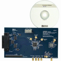
AD9858/PCBZ Summary of contents

Page 1

... Included within is information on system requirements, installing the evaluation software, menus and buttons, and window environments. Documentation for the other boards (fractional-divide loop and translation loop) is also accessible from the Design Tools section of the Analog Devices DDS homepage: www.analog.com/dds. AD9858 DDS ...

Page 2

AD9858PCB TABLE OF CONTENTS Equipment ..................................................................................... 3 Installing from the CD................................................................. 3 Installing from the Web ............................................................... 3 Main Program Window............................................................... 3 Buttons ........................................................................................... 4 Menus............................................................................................. 4 Control Window........................................................................... 5 I/O Interface.................................................................................. 6 REVISION HISTORY Revision 0: Initial Version PLL ...

Page 3

... From your browser www.analog.com/dds. 2. Click the product selection guide link. 3. Click the AD9858 link, then click the design tools link. 4. Click the install evaluation software link and follow the instructions that appear. After starting the AD9858 evaluation software, the main program window appears. At the top of the screen are the File, PC I/O, View, and Help menus and the Load Setup, Save Setup, Reset, I/O Config, and FUD buttons ...

Page 4

AD9858PCB BUTTONS The main program window has these buttons: • The Load Setup and Save Setup buttons load a setup file and save the current setup to a setup file. • The Reset button issues a master reset to the ...

Page 5

CONTROL WINDOW The control window allows the user to set many of the operating parameters of the device. In the Clock pane, the user can specify the current clock frequency supplied to the device. If the user desires, the clock ...

Page 6

AD9858PCB I/O INTERFACE This window is where the user specifies whether the evaluation board is to communicate with the AD9858 device in parallel or serial mode. In serial mode, the user can also specify LSB first or last as well ...

Page 7

PLL FAST LOCK This window is accessible from the Control window or from the View menu. The PLL Fast Lock window allows the user to enable and disable the PLL Fast Lock algorithm. When engaged, the charge pump operates in ...

Page 8

AD9858PCB PROFILES WINDOW The AD9858 has four user-defined profiles (segments of memory). Each profile can be programmed with a different frequency tuning word and phase adjustment word. As shown in Figure 12, users can click the Edit button next to ...

Page 9

FREQUENCY SWEEP SETUP DIALOG BOXES At the bottom of the Profiles window is the display for the frequency sweeping mode variables—Delta Frequency Tuning Word and Ramp Rate. Clicking the Edit button opens a dialog window that assists the user in ...

Page 10

AD9858PCB READBACK WINDOW When the READBACK button is clicked, the evaluation software polls and displays the current contents of all internal memory registers. When the CLEAR button is clicked, a master reset is issued and all internal memory registers are ...

Page 11

USING EVALUATION SOFTWARE WITH THE DAC OUTPUT BOARD As mentioned in the Circuit Overview section, the AD9858 cannot operate at speeds greater than 1 GHz. It can accept clocks from 1 GHz to 2 GHz, but the ...

Page 12

AD9858PCB ORDERING GUIDE Model Package Description AD9858/PCB Frequency Synthesizer Board © 2004 Analog Devices, Inc. All rights reserved. Trademarks and registered trademarks are the property of their respective owners. D04430-0-1/04(0) Rev Page ...

Related keywords