AD9957/PCBZ Analog Devices Inc, AD9957/PCBZ Datasheet - Page 40
AD9957/PCBZ
Manufacturer Part Number
AD9957/PCBZ
Description
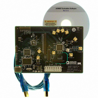
D/A Converter Evaluation Board
Manufacturer
Analog Devices Inc
Series
AgileRF™r
Datasheet
1.AD9957BSVZ-REEL.pdf
(64 pages)
Specifications of AD9957/PCBZ
Silicon Manufacturer
Analog Devices
Application Sub Type
Direct Digital Synthesizer
Kit Application Type
Clock & Timing
Silicon Core Number
AD9957
Kit Contents
Board
Main Purpose
Timing: DDS Modulators
Embedded
No
Utilized Ic / Part
AD9957
Primary Attributes
14-Bit DAC, 32-Bit Tuning Word Width
Secondary Attributes
1GHz, Graphical User Interface
Lead Free Status / RoHS Status
Lead free / RoHS Compliant
Available stocks
Company
Part Number
Manufacturer
Quantity
Price
Company:

Part Number:
AD9957/PCBZ
Manufacturer:
LT
Quantity:
962


AD9957
SYNCHRONIZATION OF MULTIPLE DEVICES
OVERVIEW
The internal clocks of the AD9957 provide the timing for the
propagation of data along the baseband signal processing path.
These internal clocks are derived from the internal system clock
(SYSCLK) and are all submultiples of the SYSCLK frequency.
The logic state of all of these clocks in aggregate during any
given SYSCLK cycle defines a unique clock state. The clock state
advances with each cycle of SYSCLK, but the sequence of clock
states is periodic. By definition, multiple devices are synchro-
nized when their clock states match and they transition between
states simultaneously. Clock synchronization allows the user to
asynchronously program multiple devices, but synchronously
activate the programming by applying a coincident I/O update
to all devices. It also allows multiple devices to operate in unison
when the parallel port is in use with either the QDUC or inter-
polating DAC mode (see Figure 59) or when the dual serial port
(BlackFin interface) is in use.
The function of the synchronization logic in the AD9957 is to
force the internal clock generator to a predefined state coincident
with an external synchronization signal applied to the SYNC_IN
pins. Forcing multiple devices to the same clock state coincident
with the same external signal is, by definition, synchronization.
Figure 54 is a block diagram of the synchronization function.
The synchronization logic consists of two independent blocks, a
sync generator and a sync receiver, both of which use the local
SYSCLK signal for internal timing.
INTERNAL
CLOCKS
PRESET VALUE
SYNC STATE
Figure 54. Synchronization Circuit Block Diagram
6
RECEIVER
SYNC
VALIDATION
HOLD VALIDATION
DELAY
SYNC
SYSCLK
RECEIVER
ENABLE
SYNC
SETUP AND
GENERATOR
4
INPUT DELAY
DETECTION
AND EDGE
SYNC
VALIDATION
CIRCUITRY
REF_CLK
DISABLE
INPUT
TIMING
SYNC
RECEIVER
DELAY
SYNC
5
5
90
91
10
12
9
7
8
SYNC_OUT
SYNC_IN
SYNC_SMP_ERR
REF_CLK
Rev. B | Page 40 of 64
The synchronization mechanism relies on the premise that the
REFCLK signal appearing at each device is edge aligned with all
others resulting from the external REFCLK distribution system
(see Figure 59).
CLOCK GENERATOR
The clock generator provides the necessary timing for the inter-
nal workings of the AD9957. The goal of the synchronization
mechanism is to force the clock generator to a known state
coincident with an external synchronization signal. The clock
generator consists of three separate clock trees (see Figure 55).
The first is a common clock generator that is active for all
programmed modes of operation (single tone, QDUC, or
interpolating DAC). The common clock generates the
SYNC_CLK signal that appears at Pin 55. The second clock
generator is active when the device is programmed for the
interpolating DAC mode or quadrature modulation mode using
the parallel data port. It uses the SYSCLK/2 output of the common
clock as its primary timing source. The third clock generator is
active when the device is programmed for quadrature modulation
mode using the BlackFin interface.
PRESET VALUE
SYNC GENERATOR
The sync generator block is shown in Figure 56. It is activated
via the Sync Generator Enable bit. It allows for one AD9957 in a
group to function as a master timing source with the remaining
devices slaved to the master.
SYNC STATE
SYSCLK
PULSE
SYNC
Figure 55. Clock Generator
COMMON CLOCK
GENERATOR
÷R
÷2
6
QUADRATURE MODULATION MODE
WITH THE BLACKFIN INTERFACE
DAC MODE OR QUADRATURE MODULATION
CLOCK GENERATOR FOR INTERPOLATING
÷R
MODE WITH THE PARALLEL DATA PORT
÷2
÷2
CLOCK GENERATOR FOR
6
÷2
÷2
÷2
÷2
PDCLK
SYNC_CLK
Related parts for AD9957/PCBZ
Image
Part Number
Description
Manufacturer
Datasheet
Request
R


Part Number:
Description:
±1.7g Dual-Axis IMEMS Accelerometer Evaluation Board
Manufacturer:
Analog Devices Inc
Datasheet:

Part Number:
Description:
Inertial Sensor Evaluation System
Manufacturer:
Analog Devices Inc
Datasheet:
Part Number:
Description:
Manufacturer:
Analog Devices Inc
Datasheet:
Part Number:
Description:
Manufacturer:
Analog Devices Inc
Datasheet:
Part Number:
Description:
Manufacturer:
Analog Devices Inc
Datasheet:
Part Number:
Description:
Manufacturer:
Analog Devices Inc
Datasheet:
Part Number:
Description:
Manufacturer:
Analog Devices Inc
Datasheet:
Part Number:
Description:
Manufacturer:
Analog Devices Inc
Datasheet:
Part Number:
Description:
Manufacturer:
Analog Devices Inc
Datasheet:
Part Number:
Description:
Manufacturer:
Analog Devices Inc
Datasheet:
Part Number:
Description:
Manufacturer:
Analog Devices Inc
Datasheet:
Part Number:
Description:
Manufacturer:
Analog Devices Inc
Datasheet: