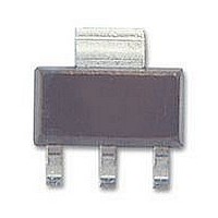
BSP171P Infineon Technologies, BSP171P Datasheet - Page 2

BSP171P
Manufacturer Part Number
BSP171P
Description
P CH MOSFET, -60V, 1.45A, SOT-223
Manufacturer
Infineon Technologies
Datasheet
1.BSP171P.pdf
(9 pages)
Specifications of BSP171P
Transistor Polarity
P Channel
Continuous Drain Current Id
1.45A
Drain Source Voltage Vds
-60V
On Resistance Rds(on)
400mohm
Rds(on) Test Voltage Vgs
-10V
Threshold Voltage Vgs Typ
-1.5V
Package
SOT-223
Vds (max)
-60.0 V
Rds (on) (max) (@10v)
300.0 mOhm
Rds (on) (max) (@4.5v)
450.0 mOhm
Rds (on) (max) (@2.5v)
-
Lead Free Status / RoHS Status
Lead free / RoHS Compliant
Available stocks
Company
Part Number
Manufacturer
Quantity
Price
Company:
Part Number:
BSP171P
Manufacturer:
INFINEON
Quantity:
30 000
Company:
Part Number:
BSP171P L6327
Manufacturer:
Infineon
Quantity:
154
Part Number:
BSP171PH6327XTSA1
Manufacturer:
INFINEON/英飞凌
Quantity:
20 000
Rev 2.3
1)
connection. PCB is vertical in still air.
Parameter
Thermal characteristics
Thermal resistance,
junction - soldering point
Thermal resistance,
junction - ambient
Electrical characteristics, at T
Static characteristics
Drain-source breakdown voltage
Gate threshold voltage
Zero gate voltage drain current
Gate-source leakage current
Drain-source on-state resistance
Transconductance
Device on 40 mm x 40 mm x 1.5 mm epoxy PCB FR4 with 6 cm
j
=25 °C, unless otherwise specified
Symbol Conditions
R
R
V
V
I
I
R
g
DSS
GSS
fs
(BR)DSS
GS(th)
thJS
thJA
DS(on)
minimal footprint,
steady state
6 cm
steady state
V
V
I
V
T
V
T
V
V
I
V
I
|V
I
D
D
D
D
j
j
GS
DS
DS
DS
GS
GS
GS
=-460 µA
=-1.5 A
=-1.9 A
=-1.5 A
=25 °C
=125 °C
DS
page 2
=V
=-60 V, V
=-60 V, V
=0 V, I
=-20 V, V
=-4.5 V,
=-10 V,
|>2|I
2
cooling area
GS
D
,
|R
D
2
=-250 µA
(one layer, 70 µm thick) copper area for drain
DS(on)max
GS
GS
DS
=0 V,
=0 V,
=0 V
1)
,
,
min.
-60
1.4
-1
-
-
-
-
-
-
-
-
Values
0.21
typ.
-1.5
-0.1
-10
-10
0.3
2.7
-
-
-
-
max.
-100
-100
0.45
110
0.3
25
70
-2
-1
-
-
BSP171P
2005-11-29
Unit
K/W
V
µA
nA
S


