APDS-9801 Avago Technologies US Inc., APDS-9801 Datasheet
APDS-9801
Specifications of APDS-9801
Available stocks


Related parts for APDS-9801


APDS-9801 Summary of contents
Page 1
... APDS-9801 Digital Proximity and Analog Ambient Light Sensor Data Sheet Description APDS-9801 is a module that integrates functions of an Analog ambient light sensor (ALS) and a proximity sensor (PS). The sensor has four chips in one small package: an ambient light sensor IC, proximity sensor signal condition- ing circuitry and a proximity sensor that includes both an emitter and detector ...
Page 2
Functional Block Diagram 8-VLED 7–PS-INTR OSC LED Control & Digital Driver Logic ³ADC Pre-Amp (12 bit) GND 1-NC 2-VDD I/O Pins Configuration Table: Pin SYMBOL Description Connect 2 VDD Power Supply Pin 3 GND Ground 2 4 ...
Page 3
Electrical & Optical Specifications (T = 25°C) A Parameter ALS Output Current ALS Dark Current ALS Peak Spectral Sensitivity ALS Light Current Ratio ALS Saturation Voltage SCL, SDA Input High Voltage SCL, SDA Input Low Voltage INTR, SDA Output Low ...
Page 4
... APDS–9801 Typical Application Circuit 1- 2-VDD C2 C1 3-GND 4-SCL 1/16W 5% R2, R3 6.8 PF 10V C1, C3 C2, C4 100 nF 10V 10 PF 10V LED C4 C3 8-VLED 7 PS-INTR APDS-9801 6-IOUT R1 5-SDA V BUS GPIO ADC MCU C5 SDA SCL ...
Page 5
Definition of timing for I C devices This section will describe the main protocol of the I2C bus. For more details and timing diagrams, please refer to the I bus specification. SDA SU;DAT f LOW ...
Page 6
I C Definition Start and Stop conditions SDA SCL S START condition Data transfer on I2C-bus SDA MSB SCL START or repeated START condition interrupt within slave A complete data transfer SDA SCL ...
Page 7
... Write Byte Protocol Slave Address Read Byte Protocol Slave Address Wr A Slave Address APDS-9801 PS slave address is 1010101 [0X55] PS-I2C Interfacing Register Address for PS: ADDRESS Register Name – Command 0h Shutdown 1h Pulse_Freq 2h Interval delay & control 3h Thres_low 4h Thres_high 5h Data_low 6h Data_high 7h interrupt Command Register The command register specifies the address of the target register for subsequence read and write operations ...
Page 8
Shutdown Register (0h Reset value: 0x0h FIELD BIT Description Shutdown 0 0 for shutdown, oscillator and analog block all turn off 1 for turn on, measurement triggered by “start measurement” bit of interval delay/control register Pulse_Freq Register (1h) ...
Page 9
Interval Delay & Control Register (2h reserved Measurement Reset value: 0x00h FIELD BIT Description Start Measurement 5 Write a “1” to this bit to enable measurement. By default this bit is ‘0’ measurement. LED Current Control ...
Page 10
ADC Data Output Register (Low byte) (5h Reset value: 0x00h FIELD BIT Description ADC output data 7:0 Lower byte of 12bits ADC output data. The ADC data are expressed as 12 bits values spread Low byte across 2 ...
Page 11
Note 1: Figure 3 Definition of transmit burst pulses st 1 burst t Pclk N x pulses Duty cycle = t/Pclk Delay = the time between the last burst pulse to the first burst pulse of the next burst Note ...
Page 12
PS – APPLICATION SOFTWARE Configuration the registers The Pulse_Freq register and Interval Delay and Control register are initialized to default values when power up. Setting these registers to desired values would be part of setup procedure. The value can be ...
Page 13
PS – Interrupts The interrupt feature of the device is simplifies and improves system efficiency by eliminating the need to poll the sensor for proximity distance value. The feature may enable at Interrupt Register. An interrupt will be happen when ...
Page 14
Read ADC Data Output Values //Read the ADC low byte channel and store at ADC_DataLow DeviceAddr = 0x55 //Set Command bit and addr of low byte of ADC Data output register Command = 0x85 ReadByte_i2c(DeviceAddr, Command, &ADC_DataLow) //Read the ADC ...
Page 15
Function Protoypes **********************************************************************/ void PXS_ShutDown(unsigned char value); void PXS_PulseFreq(unsigned char value); void PXS_PulseFreqRead(void); void PXS_IntvDelay(char value); void PXS_MeasurementEna(void); void PXS_IntvDelayRead(void); void PXS_ThresHold(unsigned char ThresholdLow, unsigned char ThresholdHigh); void PXS_ThresHoldRead(void); void PXS_IntpEna(unsigned char value); void PXS_IntpStatusRead(void); void PXS_IntpClr(void); void PXS_SoftwareReset(void); ...
Page 16
DESC: 0 for shutdown, oscillator and analog block turn off 1 for Power ON, measurement triggered by “start measurement” bit of interval delay/control register RETURNS: Nothing ***********************************************************************/ void PXS_ShutDown (unsigned char value) { unsigned char command; command = CMD| ...
Page 17
DESC: Enable measurement RETURNS: Nothing ***********************************************************************/ void PXS_MeasurementEna(void) { unsigned char command; command = CMD|ADDR_ICR; ICR_Data = 0x20 | ICR_Data; WriteByte_i2c(DeviceAddr, command, ICR_Data); } /*********************************************************************** DESC: Read back Interval delay & Control Register Value RETURNS: Interval delay & Control ...
Page 18
DESC: Read back interrupt threshold value RETURNS: Threshold Register value ***********************************************************************/ void PXS_ThresHoldRead(void) { unsigned char command; //Read back Interrupt Threshold Low Byte data command = CMD|ADDR_THRESLOW; ReadByte_i2c(DeviceAddr, command, &ReadThresholdLow); //Read back Interrupt Threshold High Byte data command = ...
Page 19
DESC: Software Reset RETURNS: Nothing ***********************************************************************/ void PXS_SoftwareReset(void) { unsigned char command; command = 0x10; Write_i2c(DeviceAddr, command); } /*********************************************************************** DESC: Read ADC Data Output Value RETURNS: ADC Low Byte and ADC HIGH Byte value ***********************************************************************/ void PXS_ADCRead(void) { unsigned ...
Page 20
... Figure 6. PS Output vs. Distance Typical Profile 700 800 900 1000 Wavelength (nm) TYPICAL IOUT VS LIGHT INTENSITY (White LED) 100 200 300 400 500 600 700 800 900 1000 LIGHT INTENSITY (LUX) APDS-9801 DISTANCE PROFILE 100 110 DISTANCE (mm) 1100 ...
Page 21
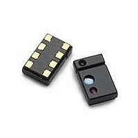
... APDS-9801 Package Outline TOP VIEW 6. LED PD ALS Ø 1. 2.50 1.60 0.75 FRONT VIEW BOTTOM VIEW 0.90 (x8 0.63 (x6) Notes: 1. All dimensions are in millimeters. Dimension tolerance is ±0.1 mm unless otherwise stated. Recommended Land Pattern 1.10 1.10 1.10 1.10 0.43 0.43 0.43 21 RIGHT VIEW 5 4 PINOUT 1 ...
Page 22
... APDS-9801 Tape & Reel Dimensions 8.00±0.10 4.00±0.10 +0.30 16.00 -0.10 3.95±0.10 8°±0° A. 60° TYP. All dimensions in millimeter. 22 2.00±0.10 Ø1.50+0.10 1.75±0.10 Ø1.50+0.25 0.30±0.02 2.05±0.00 6.20±0. 7.50±0.10 Unit Orientation in Carrier Tape ...
Page 23
... Moisture Proof Packaging All APDS-9801 options are shipped in moisture proof package. Once opened, moisture absorption begins. This part is compliant to JEDEC MSL 3. No Baking Is Necessary Baking Conditions Package Temp. In Reels 60qC In Bulk 100qC If the parts are not stored in dry conditions, they must be baked before reflow to prevent damage to the parts ...
Page 24
Recommended Reflow Profile 255 230 217 200 180 150 120 HEAT UP Process Zone Heat Up Solder Paste Dry Solder Reflow Cool Down Time maintained above liquidus point, 217°C Peak Temperature Time within 5°C ...