L3G4200DTR STMicroelectronics, L3G4200DTR Datasheet - Page 22
L3G4200DTR
Manufacturer Part Number
L3G4200DTR
Description
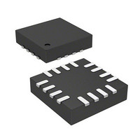
IC GYROSCOPE MEMS 3AXIS LP 16LGA
Manufacturer
STMicroelectronics
Specifications of L3G4200DTR
Package Type
LGA
Operating Supply Voltage (min)
2.4V
Operating Supply Voltage (typ)
3V
Operating Supply Voltage (max)
3.6V
Operating Temperature (min)
-40C
Operating Temperature (max)
85C
Operating Temperature Classification
Industrial
Product Depth (mm)
4mm
Product Height (mm)
1.1mm
Product Length (mm)
4mm
Mounting
Surface Mount
Pin Count
16
Lead Free Status / RoHS Status
Lead free / RoHS Compliant
Other names
497-11071-2
L3G4200DTR
L3G4200DTR
Available stocks
Company
Part Number
Manufacturer
Quantity
Price

Part Number:
L3G4200DTR
Manufacturer:
ST
Quantity:
20 000


Digital interfaces
5.1.1
22/42
I
The transaction on the bus is started through a START (ST) signal. A START condition is
defined as a HIGH to LOW transition on the data line while the SCL line is held HIGH. After
this has been transmitted by the master, the bus is considered busy. The next byte of data
transmitted after the start condition contains the address of the slave in the first 7 bits and
the eighth bit tells whether the master is receiving data from the slave or transmitting data to
the slave. When an address is sent, each device in the system compares the first 7 bits after
a start condition with its address. If they match, the device considers itself addressed by the
master.
The slave address (SAD) associated with the L3G4200D is 110100xb. The SDO pin can be
used to modify the least significant bit (LSb) of the device address. If the SDO pin is
connected to the voltage supply, LSb is ‘1’ (address 1101001b). Otherwise, if the SDO pin is
connected to ground, the LSb value is ‘0’ (address 1101000b). This solution permits the
connection and addressing of two different gyroscopes to the same I
Data transfer with acknowledge is mandatory. The transmitter must release the SDA line
during the acknowledge pulse. The receiver must then pull the data line LOW so that it
remains stable low during the HIGH period of the acknowledge clock pulse. A receiver which
has been addressed is obliged to generate an acknowledge after each byte of data
received.
The I
must be adhered to. After the START (ST) condition, a slave address is sent. Once a slave
acknowledge (SAK) has been returned, an 8-bit sub-address is transmitted. The 7 LSb
represent the actual register address while the MSB enables address auto-increment. If the
MSb of the SUB field is 1, the SUB (register address) is automatically incremented to allow
multiple data read/write.
The slave address is completed with a read/write bit. If the bit is ‘1’ (read), a REPEATED
START (SR) condition must be issued after the two sub-address bytes; if the bit is ‘0’ (write)
the master transmits to the slave with the direction unchanged.
SAD+read/write bit pattern is composed, listing all the possible configurations.
Table 13.
Table 14.
2
C operation
Master
Slave
Command
2
C embedded in the L3G4200D behaves like a slave device, and the following protocol
Read
Read
Write
Write
SAD+read/write patterns
Transfer when master is writing one byte to slave
ST
SAD[6:1]
110100
110100
110100
110100
SAD + W
Doc ID 17116 Rev 3
SAK
SAD[0] = SDO
0
0
1
1
SUB
SAK
R/W
0
0
1
1
Table 13
DATA
2
C bus.
11010001 (D1h)
11010000 (D0h)
11010011 (D3h)
11010010 (D2h)
describes how the
SAD+R/W
SAK
L3G4200D
SP
Related parts for L3G4200DTR
Image
Part Number
Description
Manufacturer
Datasheet
Request
R

Part Number:
Description:
STMicroelectronics [RIPPLE-CARRY BINARY COUNTER/DIVIDERS]
Manufacturer:
STMicroelectronics
Datasheet:
Part Number:
Description:
STMicroelectronics [LIQUID-CRYSTAL DISPLAY DRIVERS]
Manufacturer:
STMicroelectronics
Datasheet:

Part Number:
Description:
BOARD EVAL FOR MEMS SENSORS
Manufacturer:
STMicroelectronics
Datasheet:
Part Number:
Description:
NPN TRANSISTOR POWER MODULE
Manufacturer:
STMicroelectronics
Datasheet:
Part Number:
Description:
TURBOSWITCH ULTRA-FAST HIGH VOLTAGE DIODE
Manufacturer:
STMicroelectronics
Datasheet:
Part Number:
Description:
Manufacturer:
STMicroelectronics
Datasheet:
Part Number:
Description:
DIODE / SCR MODULE
Manufacturer:
STMicroelectronics
Datasheet:
Part Number:
Description:
DIODE / SCR MODULE
Manufacturer:
STMicroelectronics
Datasheet:
Part Number:
Description:
Search -----> STE16N100
Manufacturer:
STMicroelectronics
Datasheet:
Part Number:
Description:
Search ---> STE53NA50
Manufacturer:
STMicroelectronics
Datasheet:
Part Number:
Description:
NPN Transistor Power Module
Manufacturer:
STMicroelectronics
Datasheet:
Part Number:
Description:
DIODE / SCR MODULE
Manufacturer:
STMicroelectronics
Datasheet: