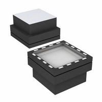
ADIS16060BCCZ Analog Devices Inc, ADIS16060BCCZ Datasheet - Page 9

ADIS16060BCCZ
Manufacturer Part Number
ADIS16060BCCZ
Description
IC GYROSCOPE YAW RATE SPI 16LGA
Manufacturer
Analog Devices Inc
Datasheet
1.ADIS16060PCBZ.pdf
(12 pages)
Specifications of ADIS16060BCCZ
Range °/s
±80°/s
Sensitivity
0.0122°/sec/LSB
Typical Bandwidth
1kHz
Voltage - Supply
4.75 V ~ 5.25 V
Current - Supply
4.3mA
Output Type
SPI
Operating Temperature
-40°C ~ 105°C
Package / Case
16-LGA
No. Of Axes
1
Sensor Case Style
LGA
No. Of Pins
16
Supply Voltage Range
4.75V To 5.25V
Operating Temperature Range
-40°C To +105°C
Msl
MSL 1 - Unlimited
Acceleration Range
2000g
Lead Free Status / RoHS Status
Lead free / RoHS Compliant
For Use With
ADIS16060/PCBZ - BOARD EVAL FOR ADIS16060
Lead Free Status / RoHS Status
Lead free / RoHS Compliant, Lead free / RoHS Compliant
THEORY OF OPERATION
The ADIS16060 operates on the principle of a resonator
gyroscope. Two polysilicon sensing structures each contain a
dither frame that is electrostatically driven to resonance. This
generates the necessary velocity element to produce a Coriolis
force while rotating. At two of the outer extremes of each frame,
orthogonal to the dither motion, are movable fingers that are
placed between fixed pickoff fingers to form a capacitive pickoff
structure that senses Coriolis motion.
The resulting signal is fed to a series of gain and demodulation
stages that produce the electrical rate signal output. The rate
signal is then converted to a digital representation of the output
on the SPI pins. The dual-sensor design provides linear acceleration
(vibration, shock) rejection. Fabricating the sensor with the signal-
conditioning electronics preserves signal integrity in noisy
environments.
The electrostatic resonator requires 14 V to 16 V for operation.
Because only 5 V is typically available in most applications, a charge
pump is included on chip. After the demodulation stage, a single-
pole, low-pass filter on the chip is used to limit high frequency
artifacts before final amplification. The frequency response is
dominated by the second low-pass filter, which is set by adding
capacitance across RATE and FILT.
ANALOG-TO-DIGITAL CONVERTER INPUT
Figure 12 shows an equivalent circuit of the input structure of
the ADIS16060 auxiliary ADC.
The two diodes, D1 and D2, provide ESD protection for the analog
inputs, AINx (AIN1 and AIN2). Care must be taken to ensure
that the analog input signal does not exceed the supply rails by
more than 0.3 V, because exceeding this level causes these diodes to
become forward-biased and to start conducting current. However,
these diodes can handle a forward-biased current of 130 mA
maximum. For instance, these conditions may eventually occur
when the input signals exceed either V
AINx
GND
Figure 12. Equivalent Analog Input Circuit
C
PIN
VDD
D1
D2
CC
R
or GND.
IN
C
IN
Rev. 0 | Page 9 of 12
During the acquisition phase, the impedance model for AINx is a
parallel combination of the capacitor C
by the series connection of R
capacitance. R
made up of some serial resistors and the on resistance of the
switches. C
ADC sampling capacitor.
During the conversion phase, when the switches are open, the
input impedance is limited to C
low-pass filter that reduces undesirable aliasing effects and
limits the noise.
When the source impedance of the driving circuit is low, the
ADC input can be driven directly. Large source impedances
significantly affect the ac performance, especially THD. The dc
performances are less sensitive to the input impedance.
RATE SENSITIVE AXIS
Figure 13. Rate Signal Increases with Clockwise Rotation
IN
is typically 30 pF and mainly functions as the
LONGITUDINAL
IN
is typically 600 Ω and is a lumped component
AXIS
1
LATERAL
AXIS
RATE
AXIS
IN
4 5
and C
PIN
. R
8
POSITIVE
MEASUREMENT
DIRECTION
IN
IN
PIN
. C
and C
and the network formed
PIN
is primarily the pin
IN
ADIS16060
make a 1-pole,


