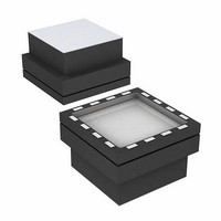
ADIS16060BCCZ Analog Devices Inc, ADIS16060BCCZ Datasheet - Page 5

ADIS16060BCCZ
Manufacturer Part Number
ADIS16060BCCZ
Description
IC GYROSCOPE YAW RATE SPI 16LGA
Manufacturer
Analog Devices Inc
Datasheet
1.ADIS16060PCBZ.pdf
(12 pages)
Specifications of ADIS16060BCCZ
Range °/s
±80°/s
Sensitivity
0.0122°/sec/LSB
Typical Bandwidth
1kHz
Voltage - Supply
4.75 V ~ 5.25 V
Current - Supply
4.3mA
Output Type
SPI
Operating Temperature
-40°C ~ 105°C
Package / Case
16-LGA
No. Of Axes
1
Sensor Case Style
LGA
No. Of Pins
16
Supply Voltage Range
4.75V To 5.25V
Operating Temperature Range
-40°C To +105°C
Msl
MSL 1 - Unlimited
Acceleration Range
2000g
Lead Free Status / RoHS Status
Lead free / RoHS Compliant
For Use With
ADIS16060/PCBZ - BOARD EVAL FOR ADIS16060
Lead Free Status / RoHS Status
Lead free / RoHS Compliant, Lead free / RoHS Compliant
TIMING SPECIFICATIONS
T
Table 2. Read/Output Sequence
Parameter
Serial Clock Frequency
Throughput Rate
MSEL1 Falling to SCLK Low
MSEL1 Falling to SCLK Rising
SCLK Falling to Data Remains Valid
MSEL1 Rising Edge to D
SCLK Falling to Data Valid
Acquisition Time
D
D
Data Setup Time
SCLK Falling Edge to MSEL2 Rising Edge
Data Hold Time
1
Timing Diagrams
Guaranteed by design. All input signals are specified with t
4.75 V to 5.25 V.
A
OUT
OUT
= 25°C, angular rate = 0°/sec, unless otherwise noted.
Fall Time
Rise Time
MSEL2
SCLK
DIN
NOTE:
THE LAST EIGHT BITS CLOCKED IN ARE LATCHED WITH THE RISING EDGE OF THE MSEL2 LINE.
MSEL1
DOUT
SCLK
NOTE:
A MINIMUM OF 20 CLOCK CYCLES ARE REQUIRED FOR 14-BIT CONVERSION.
OUT
High Impedance
1
t
CSD
t
SUCS
HIGH-Z
Figure 2. Serial Interface Timing Diagram–Read/Output Sequence (CPOL = 0, CPHA = 0)
Figure 3. Serial interface Timing–Input/Configuration Sequence (CPOL = 0, CPHA = 1)
4
5
0
t
(MSB)
EN
D13 D12 D11 D10 D9
t
CYC
R
= t
F
= 5 ns (10% to 90% of V
DB7
1
Figure Reference
See Figure 2
See Figure 2
See Figure 2
See Figure 2
See Figure 2
See Figure 2
See Figure 2
See Figure 2
See Figure 2
See Figure 3
See Figure 3
See Figure 3
DB6 DB5 DB4 DB3 DB2 DB1 DB0
t
Rev. 0 | Page 5 of 12
HDO
t
5
COMPLETE CYCLE
D8
D7
t
6
CC
D6
) and timed from a voltage level of 1.6 V. The 5 V operating range spans from
D5
D4
D3
Symbol
t
t
t
t
t
t
t
t
t
t
t
t
POWER DOWN
CYC
CSD
SUCS
HDO
DIS
EN
ACQ
F
R
5
7
6
t
D2
7
D1
D0
(LSB)
0
Min
20
5
400
5
0
4.5
t
DIS
HIGH-Z
Typ
16
14
16
11
11
5
0
t
ACQ
Max
2.9
100
0
100
50
25
25
ADIS16060
Unit
MHz
kHz
μs
ns
ns
ns
ns
ns
ns
ns
ns
ns
ns


