PIC16HV785-E/P Microchip Technology, PIC16HV785-E/P Datasheet - Page 65
PIC16HV785-E/P
Manufacturer Part Number
PIC16HV785-E/P
Description
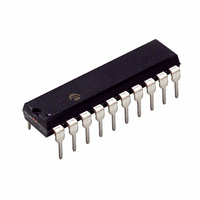
3.5KB Flash, 128 RAM, 18 I/O 20 PDIP .300in TUBE
Manufacturer
Microchip Technology
Series
PIC® 16Fr
Datasheets
1.PIC16F616T-ISL.pdf
(8 pages)
2.PIC16F785-ISS.pdf
(206 pages)
3.PIC16F785-ISS.pdf
(10 pages)
4.PIC16F785-ISS.pdf
(28 pages)
Specifications of PIC16HV785-E/P
Core Processor
PIC
Core Size
8-Bit
Speed
20MHz
Peripherals
Brown-out Detect/Reset, POR, PWM, WDT
Number Of I /o
17
Program Memory Size
3.5KB (2K x 14)
Program Memory Type
FLASH
Eeprom Size
256 x 8
Ram Size
128 x 8
Voltage - Supply (vcc/vdd)
2 V ~ 5.5 V
Data Converters
A/D 14x10b
Oscillator Type
Internal
Operating Temperature
-40°C ~ 125°C
Package / Case
20-DIP (0.300", 7.62mm)
Processor Series
PIC16H
Core
PIC
Data Bus Width
8 bit
Data Ram Size
128 B
Interface Type
RS- 232, USB
Maximum Clock Frequency
32 MHz
Number Of Programmable I/os
18
Number Of Timers
3
Maximum Operating Temperature
+ 125 C
Mounting Style
Through Hole
3rd Party Development Tools
52715-96, 52716-328, 52717-734
Development Tools By Supplier
PG164130, DV164035, DV244005, DV164005, PG164120, ICE2000, DV164120, DM163029
Minimum Operating Temperature
- 40 C
On-chip Adc
10 bit, 14 Channel
Lead Free Status / RoHS Status
Lead free / RoHS Compliant
For Use With
AC162060 - HEADER INTRFC MPLAB ICD2 20PINAC164039 - MODULE SKT PROMATE II 20DIP/SOICACICE0203 - MPLABICE 20P 300 MIL ADAPTER
Connectivity
-
Lead Free Status / Rohs Status
Details
Available stocks
Company
Part Number
Manufacturer
Quantity
Price
Company:

Part Number:
PIC16HV785-E/P
Manufacturer:
MICROCHIP
Quantity:
12 000


9.0
The Comparator module has two separate voltage
comparators: Comparator 1 (C1) and Comparator 2
(C2).
Each comparator offers the following list of features:
• Control and Configuration register
• Comparator output available externally
• Programmable output polarity
• Interrupt-on-change flags
• Wake-up from Sleep
• Configurable as feedback input to the PWM
• Programmable four input multiplexer
• Programmable two input reference selections
• Programmable speed/power
• Output synchronization to Timer1 clock input
9.1
Both comparators have separate control and Configu-
ration registers: CM1CON0 for C1 and CM2CON0 for
C2. In addition, Comparator C2 has a second control
register, CM2CON1, for synchronization control and
simultaneous reading of both comparator outputs.
9.1.1
The CM1CON0 register (shown in Register 9-1)
contains the control and Status bits for the following:
• Comparator enable
• Comparator input selection
• Comparator reference selection
• Output mode
• Comparator speed
Setting C1ON (CM1CON0<7>) enables Comparator
C1 for operation.
Bits C1CH<1:0> of the CM1CON0 Register select the
comparator input from the four analog pins AN<7:5,1>.
© 2008 Microchip Technology Inc.
(Comparator C2 only)
Note:
COMPARATOR MODULE
Control Registers
COMPARATOR C1 CONTROL
REGISTER
To use AN<7:5,1> as analog inputs the
appropriate bits must be programmed to
‘1’ in the ANSEL0 register.
Setting C1R of the CM1CON0 Register selects the
C1V
module as the reference voltage for the comparator.
Clearing C1R selects the C1IN+ input on the RA0/AN0/
C1IN+/ICSPDAT pin.
The output of the comparator is available internally via
the C1OUT flag of the CM1CON0 Register. To make
the output available for an external connection, the
C1OE bit of the CM1CON0 Register must be set.
The polarity of the comparator output can be inverted
by setting the C1POL bit of the CM1CON0 Register.
Clearing C1POL results in a non-inverted output.
A complete table showing the output state versus input
conditions and the polarity bit is shown in Table 9-1.
TABLE 9-1:
C1SP of the CM1CON0 Register configures the speed
of the comparator. When C1SP is set, the comparator
operates at its normal speed. Clearing C1SP operates
the comparator in a slower, low-power mode.
Input Condition
Note 1: The internal output of the comparator is
C1VN > C1VP
C1VN < C1VP
C1VN > C1VP
C1VN < C1VP
REF
PIC16F785/HV785
2: The C1 interrupt will operate correctly
3: To output C1 on RA2/AN2/T0CKI/INT/
output of the comparator voltage reference
latched at the end of each instruction
cycle. External outputs are not latched.
with C1OE set or cleared.
C1OUT:(C1OE = 1) and (C1ON = 1) and
(TRISA<2> = 0).
C1 OUTPUT STATE VERSUS
INPUT CONDITIONS
C1POL
0
0
1
1
DS41249E-page 63
C1OUT
0
1
1
0
Related parts for PIC16HV785-E/P
Image
Part Number
Description
Manufacturer
Datasheet
Request
R

Part Number:
Description:
Manufacturer:
Microchip Technology Inc.
Datasheet:
Part Number:
Description:
Manufacturer:
Microchip Technology Inc.
Datasheet:
Part Number:
Description:
Manufacturer:
Microchip Technology Inc.
Datasheet:
Part Number:
Description:
Manufacturer:
Microchip Technology Inc.
Datasheet:
Part Number:
Description:
Manufacturer:
Microchip Technology Inc.
Datasheet:
Part Number:
Description:
Manufacturer:
Microchip Technology Inc.
Datasheet:
Part Number:
Description:
Manufacturer:
Microchip Technology Inc.
Datasheet:
Part Number:
Description:
Manufacturer:
Microchip Technology Inc.
Datasheet: