PIC16HV785-E/P Microchip Technology, PIC16HV785-E/P Datasheet - Page 162
PIC16HV785-E/P
Manufacturer Part Number
PIC16HV785-E/P
Description
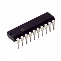
3.5KB Flash, 128 RAM, 18 I/O 20 PDIP .300in TUBE
Manufacturer
Microchip Technology
Series
PIC® 16Fr
Datasheets
1.PIC16F616T-ISL.pdf
(8 pages)
2.PIC16F785-ISS.pdf
(206 pages)
3.PIC16F785-ISS.pdf
(10 pages)
4.PIC16F785-ISS.pdf
(28 pages)
Specifications of PIC16HV785-E/P
Core Processor
PIC
Core Size
8-Bit
Speed
20MHz
Peripherals
Brown-out Detect/Reset, POR, PWM, WDT
Number Of I /o
17
Program Memory Size
3.5KB (2K x 14)
Program Memory Type
FLASH
Eeprom Size
256 x 8
Ram Size
128 x 8
Voltage - Supply (vcc/vdd)
2 V ~ 5.5 V
Data Converters
A/D 14x10b
Oscillator Type
Internal
Operating Temperature
-40°C ~ 125°C
Package / Case
20-DIP (0.300", 7.62mm)
Processor Series
PIC16H
Core
PIC
Data Bus Width
8 bit
Data Ram Size
128 B
Interface Type
RS- 232, USB
Maximum Clock Frequency
32 MHz
Number Of Programmable I/os
18
Number Of Timers
3
Maximum Operating Temperature
+ 125 C
Mounting Style
Through Hole
3rd Party Development Tools
52715-96, 52716-328, 52717-734
Development Tools By Supplier
PG164130, DV164035, DV244005, DV164005, PG164120, ICE2000, DV164120, DM163029
Minimum Operating Temperature
- 40 C
On-chip Adc
10 bit, 14 Channel
Lead Free Status / RoHS Status
Lead free / RoHS Compliant
For Use With
AC162060 - HEADER INTRFC MPLAB ICD2 20PINAC164039 - MODULE SKT PROMATE II 20DIP/SOICACICE0203 - MPLABICE 20P 300 MIL ADAPTER
Connectivity
-
Lead Free Status / Rohs Status
Details
Available stocks
Company
Part Number
Manufacturer
Quantity
Price
Company:

Part Number:
PIC16HV785-E/P
Manufacturer:
MICROCHIP
Quantity:
12 000


PIC16F785/HV785
FIGURE 19-9:
TABLE 19-16: PIC16F785/HV785 A/D CONVERSION REQUIREMENTS
DS41249E-page 160
130
130
131
132
134
Note 1:
Param
No.
Note 1:
A/D DATA
2:
SAMPLE
A/D CLK
*
†
BSF ADCON0, GO
ADRES
T
T
T
T
T
ADIF
AD
AD
CNV
ACQ
GO
These parameters are characterized but not tested.
Data in ‘Typ’ column is at 5.0V, 25°C unless otherwise stated. These parameters are for design guidance only and are
not tested.
ADRESH and ADRESL registers may be read on the following T
See Section 12.2 “A/D Acquisition Requirements” for minimum conditions.
Sym
GO
Q4
If the A/D clock source is selected as RC, a time of T
SLEEP instruction to be executed.
134
A/D Clock Period
A/D Internal RC
Oscillator Period
Conversion Time (not
including
Acquisition Time)
Acquisition Time
Q4 to A/D Clock Start
132
Characteristic
PIC16F785/HV785 A/D CONVERSION TIMING (NORMAL MODE)
(1)
(T
OSC
/2)
(Note 2)
(1)
Min
3.0*
3.0*
2.0*
9
1.6
—
5*
—
OLD_DATA
8
T
Typ†
OSC
11.5
6.0
4.0
SAMPLING STOPPED
—
—
11
—
131
7
/2
CY
6
is added before the A/D clock starts. This allows the
Max
130
6.0*
9.0*
—
—
—
—
—
—
CY
3
cycle.
Units
T
μs
μs
μs
μs
μs
μs
—
AD
2
T
T
ADCS<1:0> = 11 (RC mode)
At V
At V
Set GO bit to new data in A/D result
register
The minimum time is the amplifier settling
time. This may be used if the “new” input
voltage has not changed by more than 1
LSb (i.e., 4.1 mV @ 4.096V) from the last
sampled voltage (as stored on C
If the A/D clock source is selected as
RC, a time of T
A/D clock starts. This allows the SLEEP
instruction to be executed.
OSC
OSC
1
DD
DD
-based, V
-based, V
© 2008 Microchip Technology Inc.
= 2.5V
= 5.0V
0
Conditions
REF
REF
CY
is added before the
NEW_DATA
≥ 3.0V
full range
DONE
1 T
CY
1 T
CY
HOLD
).
Related parts for PIC16HV785-E/P
Image
Part Number
Description
Manufacturer
Datasheet
Request
R

Part Number:
Description:
Manufacturer:
Microchip Technology Inc.
Datasheet:
Part Number:
Description:
Manufacturer:
Microchip Technology Inc.
Datasheet:
Part Number:
Description:
Manufacturer:
Microchip Technology Inc.
Datasheet:
Part Number:
Description:
Manufacturer:
Microchip Technology Inc.
Datasheet:
Part Number:
Description:
Manufacturer:
Microchip Technology Inc.
Datasheet:
Part Number:
Description:
Manufacturer:
Microchip Technology Inc.
Datasheet:
Part Number:
Description:
Manufacturer:
Microchip Technology Inc.
Datasheet:
Part Number:
Description:
Manufacturer:
Microchip Technology Inc.
Datasheet: