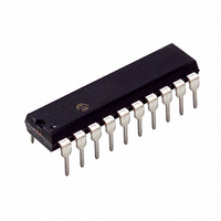
PIC16HV785-E/P Microchip Technology, PIC16HV785-E/P Datasheet - Page 53

PIC16HV785-E/P
Manufacturer Part Number
PIC16HV785-E/P
Description
3.5KB Flash, 128 RAM, 18 I/O 20 PDIP .300in TUBE
Manufacturer
Microchip Technology
Series
PIC® 16Fr
Datasheets
1.PIC16F616T-ISL.pdf
(8 pages)
2.PIC16F785-ISS.pdf
(206 pages)
3.PIC16F785-ISS.pdf
(10 pages)
4.PIC16F785-ISS.pdf
(28 pages)
Specifications of PIC16HV785-E/P
Core Processor
PIC
Core Size
8-Bit
Speed
20MHz
Peripherals
Brown-out Detect/Reset, POR, PWM, WDT
Number Of I /o
17
Program Memory Size
3.5KB (2K x 14)
Program Memory Type
FLASH
Eeprom Size
256 x 8
Ram Size
128 x 8
Voltage - Supply (vcc/vdd)
2 V ~ 5.5 V
Data Converters
A/D 14x10b
Oscillator Type
Internal
Operating Temperature
-40°C ~ 125°C
Package / Case
20-DIP (0.300", 7.62mm)
Processor Series
PIC16H
Core
PIC
Data Bus Width
8 bit
Data Ram Size
128 B
Interface Type
RS- 232, USB
Maximum Clock Frequency
32 MHz
Number Of Programmable I/os
18
Number Of Timers
3
Maximum Operating Temperature
+ 125 C
Mounting Style
Through Hole
3rd Party Development Tools
52715-96, 52716-328, 52717-734
Development Tools By Supplier
PG164130, DV164035, DV244005, DV164005, PG164120, ICE2000, DV164120, DM163029
Minimum Operating Temperature
- 40 C
On-chip Adc
10 bit, 14 Channel
Lead Free Status / RoHS Status
Lead free / RoHS Compliant
For Use With
AC162060 - HEADER INTRFC MPLAB ICD2 20PINAC164039 - MODULE SKT PROMATE II 20DIP/SOICACICE0203 - MPLABICE 20P 300 MIL ADAPTER
Connectivity
-
Lead Free Status / Rohs Status
Details
Available stocks
Company
Part Number
Manufacturer
Quantity
Price
Company:
Part Number:
PIC16HV785-E/P
Manufacturer:
MICROCHIP
Quantity:
12 000
- PIC16F616T-ISL PDF datasheet
- PIC16F785-ISS PDF datasheet #2
- PIC16F785-ISS PDF datasheet #3
- PIC16F785-ISS PDF datasheet #4
- Current page: 53 of 206
- Download datasheet (4Mb)
6.0
The Timer1 module is the 16-bit counter of the
PIC16F785/HV785. Figure 6-1 shows the basic block
diagram of the Timer1 module. Timer1 has the follow-
ing features:
• 16-bit timer/counter (TMR1H:TMR1L)
• Readable and writable
• Internal or external clock selection
• Synchronous or asynchronous operation
• Interrupt on overflow from FFFFh to 0000h
• Wake-up upon overflow (Asynchronous mode)
• Optional external enable input:
• Optional LP oscillator
FIGURE 6-1:
© 2008 Microchip Technology Inc.
- Selectable gate source; T1G or C2 output
- Selectable gate polarity (T1GINV)
Without CLKOUT
(T1GSS)
RA5/T1CKI/OSC1/CLKIN
RA4/AN3/T1G/OSC2/CLKOUT
Note 1: Timer1 increments on the rising edge.
INTOSC
TIMER1 MODULE WITH GATE
CONTROL
LP
Sleep
*
2: SYNCC2OUT is the synchronized output from Comparator 2 (See Figure 9-2 on 66).
ST Buffer is low power type when using LP OSC, or high-speed type when using T1CKI.
Set flag bit
TMR1IF on
Overflow
T1OSCEN
TIMER1 ON THE PIC16F785/HV785 BLOCK DIAGRAM
TMR1H
Oscillator
TMR1
(1)
TMR1L
*
Internal
Clock
F
OSC
Q
EN
D
/4
The Timer1 Control register (T1CON), shown in
Register 6-1, is used to enable/disable Timer1 and
select the various features of the Timer1 module.
TMR1CS
1
0
To C2 Comparator Module
TMR1 Clock
PIC16F785/HV785
T1CKPS<1:0>
T1SYNC
SYNCC2OUT
Prescaler
1, 2, 4, 8
0
1
2
TMR1ON
TMR1GE
TMR1ON
TMR1GE
(2)
Synchronized
clock input
T1GSS
Sleep input
Synchronize
1
0
det
DS41249E-page 51
T1GINV
Related parts for PIC16HV785-E/P
Image
Part Number
Description
Manufacturer
Datasheet
Request
R

Part Number:
Description:
Manufacturer:
Microchip Technology Inc.
Datasheet:

Part Number:
Description:
Manufacturer:
Microchip Technology Inc.
Datasheet:

Part Number:
Description:
Manufacturer:
Microchip Technology Inc.
Datasheet:

Part Number:
Description:
Manufacturer:
Microchip Technology Inc.
Datasheet:

Part Number:
Description:
Manufacturer:
Microchip Technology Inc.
Datasheet:

Part Number:
Description:
Manufacturer:
Microchip Technology Inc.
Datasheet:

Part Number:
Description:
Manufacturer:
Microchip Technology Inc.
Datasheet:

Part Number:
Description:
Manufacturer:
Microchip Technology Inc.
Datasheet:


