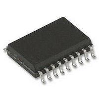
ST62T15CM6 STMicroelectronics, ST62T15CM6 Datasheet - Page 90

ST62T15CM6
Manufacturer Part Number
ST62T15CM6
Description
8BIT MCU OTP 2K, SMD, 62T15, SOIC20
Manufacturer
STMicroelectronics
Datasheet
1.ST62T15CB6.pdf
(105 pages)
Specifications of ST62T15CM6
Controller Family/series
ST6
Core Size
8bit
No. Of I/o's
20
Program Memory Size
2KB
Ram Memory Size
64Byte
Cpu Speed
8MHz
Oscillator Type
External Only
No. Of Timers
1
Digital Ic Case
RoHS Compliant
Peripherals
ADC,
Rohs Compliant
No
Processor Series
ST62T1x
Core
ST6
Data Bus Width
8 bit
Program Memory Type
EPROM
Data Ram Size
64 B
Maximum Clock Frequency
8 MHz
Number Of Programmable I/os
20
Number Of Timers
2
Operating Supply Voltage
3 V to 6 V
Maximum Operating Temperature
+ 85 C
Mounting Style
SMD/SMT
Package / Case
SOP-28
Development Tools By Supplier
ST62GP-EMU2, ST62E2XC-EPB/110, ST62E6XC-EPB/US, STREALIZER-II
Minimum Operating Temperature
- 40 C
On-chip Adc
8 bit
Lead Free Status / Rohs Status
In Transition
Available stocks
Company
Part Number
Manufacturer
Quantity
Price
Company:
Part Number:
ST62T15CM6
Manufacturer:
STM
Quantity:
2 508
Part Number:
ST62T15CM6
Manufacturer:
ST
Quantity:
20 000
ST6215C/ST6225C
8-BIT ADC CHARACTERISTICS (Cont’d)
ADC Accuracy
Notes:
1. Negative injection disturbs the analog performance of the device. In particular, it induces leakage currents throughout
2. Data based on characterization results over the whole temperature range, monitored in production.
Figure 73. ADC Accuracy Characteristics
Note: ADC not present on some devices. See device summary on page 1.
90/105
1
Symbol
255
254
253
the device including the analog inputs. To avoid undesirable effects on the analog functions, care must be taken:
- Analog input pins must have a negative injection less than 1mA (assuming that the impedance of the analog voltage
is lower than the specified limits).
- Pure digital pins must have a negative injection less than 1mA. In addition, it is recommended to inject the current as
far as possible from the analog input pins.
|E
|E
|E
7
6
5
4
3
2
1
E
E
0
V
O
G
D
T
L
SSA
|
|
|
Digital Result ADCDR
1
1LSB
Total unadjusted error
Offset error
Gain Error
Differential linearity error
Integral linearity error
E
O
2
IDE AL
3
1)
Parameter
=
1)
4
V
---------------------------------------- -
DDA
5
256
1 LSB
–
V
1)
E
1)
SSA
6
T
IDEAL
1)
E
7
L
(2)
E
D
Conditions
f
253 254 255 256
OSC
(3)
V
DD
=8MHz
=5V
(1)
2)
E
G
V
DDA
Min
(1) Example of an actual transfer curve
(2) The ideal transfer curve
(3) End point correlation line
E
between the actual and the ideal transfer curves.
E
transition and the first ideal one.
E
transition and the last actual one.
E
between actual steps and the ideal one.
E
between any actual transition and the end point
correlation line.
T
O
G
D
L
=Total Unadjusted Error: maximum deviation
=Integral Linearity Error: maximum deviation
=Offset Error: deviation between the first actual
=Gain Error: deviation between the last ideal
=Differential Linearity Error: maximum deviation
V
in
(LSB
-0.31
Typ.
0.72
0.54
1.2
IDEAL
)
2, fosc>1.2MHz
4, fosc>32KHz
Max
Unit
LSB


