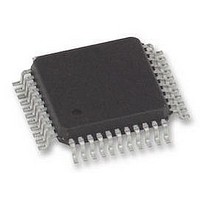
FM6124-QG Ramtron, FM6124-QG Datasheet - Page 28

FM6124-QG
Manufacturer Part Number
FM6124-QG
Description
FRAM, 24KB, EVENT DATA REC, QFP44
Manufacturer
Ramtron
Datasheet
1.FM6124-QG.pdf
(53 pages)
Specifications of FM6124-QG
Memory Size
24KB
Nvram Features
RTC
Supply Voltage Range
3V To 3.6V
Memory Case Style
QFP
No. Of Pins
44
Operating Temperature Range
-40°C To +85°C
Package / Case
QFP
Interface
I2C
Memory
RoHS Compliant
Interface Type
I2C, Serial, 2-Wire
Rohs Compliant
Yes
Access Time
100 KBPs
Operating Supply Voltage
3 V to 3.6 V
Mounting Style
SMD/SMT
Lead Free Status / Rohs Status
Details
Available stocks
Company
Part Number
Manufacturer
Quantity
Price
Company:
Part Number:
FM6124-QG
Manufacturer:
ABOV
Quantity:
3 000
Rev. 4.0 (EOL)
July 2010
0x2C
Event Code
[7:0]
0x2B
0x2A
# Unread
Event
Counter
[15:0]
0x29
P11-P4
0x28
P3-P0
0x27
NBEV
SNAP
0x26
P11-P4
0x25
P3 – P0
Event Data Code
An Event code is associated with Each recorded event.
The table below shows the association between the Events and their corresponding Event Code.
Unread Events Counter MSB
Unread Events Counter LSB
This 16-bit register contains the number of unread Event held in the FM6124 Event Buffer F-RAM memory.
This value corresponds to the distance between WP and RP pointers.
A snapshot of the internal Unread Event Counter must be performed before reading this register.
This is done by writing 0x02 into the register located at address 27h
Pin Pass-Through B
Read Only: This register contains the Input pin logic level at the moment the snapshot was performed
Pin Pass-Through A
Read Only: This register contains the Input pin logic level at the moment the snapshot was performed
Pin State – #Events Snapshot
register and write the corresponding input logic level into the Register 2Ah and 2Bh
Write Only: Writing a 1 into the SNAP will perform a snapshot read of all 12 Input of the FM6124 and write the
corresponding input logic level into the Register 28h and 29h
Pin Event Enable B
Pin Event Enable
0: Event detection on the corresponding input pin is disabled
1: Event detection on the corresponding input pin is Activated
Pin Event Enable A
Pin Event Enable
0: Event detection on the corresponding input pin is disabled
1: Event detection on the corresponding input pin is Activated
Write Only: Writing a 1 into the NBEVP will perform a snapshot read of the internal unread Events Counter
Event
EV_PIN0_FALL
EV_PIN0_RISE
EV_PIN1_FALL
EV_PIN1_RISE
EV_PIN2_FALL
EV_PIN2_RISE
EV_PIN3_FALL
EV_PIN3_RISE
EV_PIN4_FALL
EV_PIN4_RISE
EV_PIN5_FALL
EV_PIN5_RISE
P11
P11
D7
D7
D7
D7
D7
D7
D7
D7
P10
P10
D6
D6
D6
D6
D6
D6
D6
D6
Reserved
Reserved
Event Code
0x08
0x09
0x0A
0x0B
0x0C
0x0D
0x0E
0x0F
0x10
0x11
0x12
0x13
D5
D5
D5
D5
D5
D5
D5
D5
P9
P9
Reserved
Number of Unread Event Counter[15:8]
Number of Unread Event Counter[7:0]
D4
D4
D4
D4
D4
D4
D4
D4
P8
P8
Event Code[7:0]
Event
EV_PIN6_FALL
EV_PIN6_RISE
EV_PIN7_FALL
EV_PIN7_RISE
EV_PIN8_FALL
EV_PIN8_RISE
EV_PIN9_FALL
EV_PIN9_RISE
EV_PIN10_FALL
EV_PIN10_RISE
EV_PIN11_FALL
EV_PIN11_RISE
D3
D3
D3
D3
D3
D3
D3
D3
P7
P3
P7
P3
D2
D2
D2
D2
D2
D2
D2
D2
P6
P2
P6
P2
Event Code
0x14
0x15
0x16
0x17
0x18
0x19
0x1A
0x1B
0x1C
0x1D
0x1E
0x1F
FM6124 Event Data Recorder
NBEV
D1
D1
D1
D1
D1
D1
D1
D1
P5
P1
P5
P1
Page 28 of 53
SNAP
D0
D0
D0
D0
D0
D0
D0
D0
P4
P0
P4
P0


