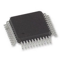
FM6124-QG Ramtron, FM6124-QG Datasheet - Page 12

FM6124-QG
Manufacturer Part Number
FM6124-QG
Description
FRAM, 24KB, EVENT DATA REC, QFP44
Manufacturer
Ramtron
Datasheet
1.FM6124-QG.pdf
(53 pages)
Specifications of FM6124-QG
Memory Size
24KB
Nvram Features
RTC
Supply Voltage Range
3V To 3.6V
Memory Case Style
QFP
No. Of Pins
44
Operating Temperature Range
-40°C To +85°C
Package / Case
QFP
Interface
I2C
Memory
RoHS Compliant
Interface Type
I2C, Serial, 2-Wire
Rohs Compliant
Yes
Access Time
100 KBPs
Operating Supply Voltage
3 V to 3.6 V
Mounting Style
SMD/SMT
Lead Free Status / Rohs Status
Details
Available stocks
Company
Part Number
Manufacturer
Quantity
Price
Company:
Part Number:
FM6124-QG
Manufacturer:
ABOV
Quantity:
3 000
Event Memory/User F-RAM Memory Size
Configuration
The FM6124 contains a total of 32KBytes (256Kb) of F-
RAM memory on chip. The F-RAM memory can be
configured to serve for both Event Recording and for User
Data saving. The portion of the memory reserved for User
Data is defined through register and occupies the lower
portion of the address range.
The upper portion of the F-RAM addresses is used to store
Event type and timestamp information. The data associated
with Event is accessible only through I
registers.
The boundary between User FRAM and Event Recording
FRAM is adjusted through configuration register in the
Event recording portion of the device. The memory
boundary can be changed at any time, however each time it
is changed the entire F-RAM memory (Event Recording/
User Data) will be erased.
The portion of the F-RAM defined as User Memory Data
memory use consistent two-byte addressing for the
memory device rendering it code compatible to the
standalone memory counterparts, such as the FM24xx but
with the ability to be configured up to 24KB in size.
Up to 4000 events can be saved in the FM6124 Event
buffer F-RAM memory. A percentage of the F-RAM can
also be configured as User F-RAM that is accessed like
standard I
device ID for User F-RAM access.
The EBUFSIZE[1:0] portion of the Event Data Recorder
control register (address 0x20) defines the portion of
memory reserved for Event recording and User F-RAM
size as shown in the table below:
When the entire F-RAM memory is reserved for Event
recording, there will be no User F-RAM available and the
FM6124 will stop acknowledging on any I
initiated with F-RAM / EEPROM device ID.
This allows one to share the I
FM6124 and up to eight I
Event Buffer Architecture
The structure of the Event Buffer memory is analogue to a
Circular buffer: Initially the Event data will be stored
from a base address that we will call FP, for First pointer
Rev. 4.0 (EOL)
July 2010
EBUFSIZE[1:0]
00
01
10
11
2
C based F-RAM and using a dedicated I
Max number of Events
4000
3000
2000
1000
2
C based memory devices.
2
C bus between up to four
User F-RAM size
0
64 Kb
128 Kb
192 Kb
2
C transactions
2
C Mapped
2
C
and up to the maximum number of Event that the FM6124
have been configured to hold. We will call this address
Nmax.
Initially the FP pointer is likely to be at lowest possible F-
RAM address. However, when the event buffer is full the
address of the FP pointer will be incremented for each new
event recorded.
Event Buffer Pointers
The management of Event recording and retrieval is
handled using nonvolatile F-RAM based virtual pointers.
The addresses where these pointers point to are not directly
accessible through the I
provides commands to control the way those pointers
behave.
Four Pointers are defined:
First pointer
The FP pointer is the reference pointer which is fixed for a
given Event recorder configuration.
The first pointer actually indicates the position of oldest
event recorded and it is used as a reference.
movements of the RP and WP pointers are referenced to
the FP pointer.
Each time the FM6124 configuration is changed through
EBUFSIZE[1:0] register, the position of FP will be reset to
the lowest F-RAM address and it will not move until the
Event buffer is filled.
When the number of event recorded exceeds the buffer
capacity, the FP pointer address will be incremented each
FP:
RP:
SP:
WP:
F
IGURE
First pointer
Read Pointer
Stream Pointer
Write pointer
14. E
2
VENT
C interface however the FM6124
B
UFFER OVERVIEW
Page 12 of 53
The


