FM6124-QG Ramtron, FM6124-QG Datasheet - Page 19
FM6124-QG
Manufacturer Part Number
FM6124-QG
Description
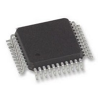
FRAM, 24KB, EVENT DATA REC, QFP44
Manufacturer
Ramtron
Datasheet
1.FM6124-QG.pdf
(53 pages)
Specifications of FM6124-QG
Memory Size
24KB
Nvram Features
RTC
Supply Voltage Range
3V To 3.6V
Memory Case Style
QFP
No. Of Pins
44
Operating Temperature Range
-40°C To +85°C
Package / Case
QFP
Interface
I2C
Memory
RoHS Compliant
Interface Type
I2C, Serial, 2-Wire
Rohs Compliant
Yes
Access Time
100 KBPs
Operating Supply Voltage
3 V to 3.6 V
Mounting Style
SMD/SMT
Lead Free Status / Rohs Status
Details
Available stocks
Company
Part Number
Manufacturer
Quantity
Price
Company:

Part Number:
FM6124-QG
Manufacturer:
ABOV
Quantity:
3 000


occurred as V
started while V
internally.
Table 2 below shows how bits VTP(1:0) control the trip
point of the low-V
18h, bits 0 and 1. The reset pin will drive low when V
below the selected V
reset operation in response to a low V
A watchdog timer can also be used to drive an active reset
signal. The watchdog is a free-running programmable
timer. The timeout period can be software programmed
from 60 ms to 1.8 seconds in 60 ms increments via a 5-bit
nonvolatile setting (register 0Ch).
The watchdog also incorporates a window timer feature
that allows a delayed start. The starting time and ending
time defines the window and each may be set
independently. The starting time has 25 ms resolution and
0 ms to 775 ms range.
Rev. 4.0 (EOL)
July 2010
VDD
VTP
RST
Timebase
Table 2.
100 ms
clock
DD
VTP Setting
F
F
IGURE
dropped below V
IGURE
2.75V
DD
2.6V
2.9V
3.0V
DD
Timer Settings
Down Counter
is above V
TP
Watchdog
21. W
reset. They are located in register
20. L
voltage. Figure 20 illustrates the
OW
WR3-0 = 1010b
ATCHDOG TIMER
VTP1
VDD R
0
0
1
1
TP
TP
. A memory operation
DD
WDE
ESET
VTP0
to restart
will be completed
.
0
1
0
1
tRPU
RSTB
DD
is
The watchdog EndTime value is located in register 0Ch,
bits 4-0, the watchdog enable is bit 7. The watchdog is
restarted by writing the pattern 1010b to the lower nibble
of register 0Ah. Writing the correct pattern will also cause
the timer to load new timeout values. Writing other
patterns to this address will not affect its operation. Note
the watchdog timer is free-running. Prior to enabling it,
users should restart the timer as described above. This
assures that the full timeout is provided immediately after
enabling. The watchdog is disabled when V
V
zeroes (00000b) disables the timer to save power. The
listing below summarizes the watchdog bits.
Watchdog StartTime
Watchdog EndTime
Watchdog Enable
Watchdog Restart
Watchdog Flags
The programmed StartTime value is a guaranteed
maximum time while the EndTime value is a guaranteed
minimum time, and both vary with temperature and V
voltage. The watchdog has two additional controls
associated with its operation. The nonvolatile enable bit
WDE allows the RSTB to go active if the watchdog
reaches the timeout without being restarted. If a reset
occurs, the timer will restart on the rising edge of the reset
pulse. If WDE is not enabled, the watchdog timer still runs
but has no effect on RSTB. The second control is a nibble
that restarts the timer, thus preventing a reset. The timer
should be restarted after changing the timeout value.
This procedure must be followed to properly load the
watchdog registers:
The restart command in step 3 must be issued before t
which was programmed in step 2. The window timer starts
counting when the restart command is issued.
Watchdog
TP
Restart
.
1.
2.
3.
RST
Note setting the EndTime timeout setting to all
Write the StartTime value
Write the EndTime value and WDE=1 0Ch
Issue a Restart command
F
Start
Time
IGURE
Window
WDST4-0 0Bh, bits 4-0
WDET4-0 0Ch, bits 4-0
WDE
WR3-0
EWDF,
LWDF
22. W
INDOW TIMER
End
Time
0Ch, bit 7
0Ah, bits 3-0
09h, bit 7
09h, bit 6
100 ms (max)
Page 19 of 53
DD
Address
0Bh
0Ah
drops below
DOG2
DD
,
Related parts for FM6124-QG
Image
Part Number
Description
Manufacturer
Datasheet
Request
R

Part Number:
Description:
Event Data Recorder With F-ram
Manufacturer:
Ramtron Corporation
Datasheet:

Part Number:
Description:
SOP28
Manufacturer:
Ramtron
Datasheet:
Part Number:
Description:
SOP-28
Manufacturer:
Ramtron
Datasheet:
Part Number:
Description:
SOP-28
Manufacturer:
Ramtron
Datasheet:
Part Number:
Description:
SOP-28
Manufacturer:
Ramtron
Datasheet:
Part Number:
Description:
TSOP44
Manufacturer:
Ramtron
Datasheet:
Part Number:
Description:
SOP8
Manufacturer:
Ramtron
Datasheet:
Part Number:
Description:
SOP8
Manufacturer:
Ramtron
Datasheet: