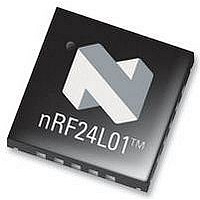
NRF24L01G NORDIC SEMICONDUCTOR, NRF24L01G Datasheet - Page 60

NRF24L01G
Manufacturer Part Number
NRF24L01G
Description
IC, RF TRANSCEIVER, 2.4-2.4835GHZ QFN-20
Manufacturer
NORDIC SEMICONDUCTOR
Datasheet
1.NRF24L01G.pdf
(74 pages)
Specifications of NRF24L01G
Transmitting Current
11.3mA
Data Rate
2Mbps
Frequency Range
2.4GHz To 2.4835GHz
Modulation Type
GFSK
Sensitivity Dbm
-82dBm
Rf Ic Case Style
QFN
No. Of Pins
20
Sensitivity (dbm)
-82dBm
Supply Voltage Range
1.9V To 3.6V
Rohs Compliant
Yes
Lead Free Status / RoHS Status
Lead free / RoHS Compliant
The nRF24L01 crystal oscillator is amplitude regulated. It is recommended to use an input signal larger
than 0.4V-peak to achieve low current consumption and good signal-to-noise ratio when using an external
clock. XC2 is not used and can be left as an open pin when clocked externally.
10.4
A well designed PCB is necessary to achieve good RF performance. A poor layout can lead to loss of per-
formance or functionality. A fully qualified RF-layout for the nRF24L01 and its surrounding components,
including matching networks, can be downloaded from www.nordicsemi.no.
A PCB with a minimum of two layers including a ground plane is recommended for optimum performance.
The nRF24L01 DC supply voltage should be decoupled as close as possible to the VDD pins with high per-
formance RF capacitors, see
tor (for example, 4.7μF ceramic) in parallel with the smaller value capacitors. The nRF24L01 supply
voltage should be filtered and routed separately from the supply voltages of any digital circuitry.
Long power supply lines on the PCB should be avoided. All device grounds, VDD connections and VDD
bypass capacitors must be connected as close as possible to the nRF24L01 IC. For a PCB with a topside
RF ground plane, the VSS pins should be connected directly to the ground plane. For a PCB with a bottom
ground plane, the best technique is to have via holes as close as possible to the VSS pads. A minimum of
one via hole should be used for each VSS pin.
Full swing digital data or control signals should not be routed close to the crystal or the power supply lines.
The exposed die attach pad is a ground pad connected to the IC substrate die ground and is intentionally
not used in our layouts. It is recommended to keep it unconnected.
Revision 2.0
PCB layout and decoupling guidelines
Table 26. on page
Figure 28. Principle of crystal oscillator
Vss
ESD
Vdd
XC1
Page 60 of 74
69. It is preferable to mount a large surface mount capaci-
current source
Current starved
XO_OUT
full swing
XC2
Amplitude
controlled
Sine to
Buffer:
XOSC core
nRF24L01 Product Specification
inverter:
ESD
Vdd
Vss


