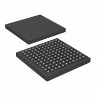
PIC32MX795F512L-80I/BG Microchip Technology, PIC32MX795F512L-80I/BG Datasheet - Page 8

PIC32MX795F512L-80I/BG
Manufacturer Part Number
PIC32MX795F512L-80I/BG
Description
IC, 32BIT MCU, PIC32, 80MHZ, BGA-100
Manufacturer
Microchip Technology
Series
PIC® 32MXr
Datasheets
1.PIC32MX320F032H-40IPT.pdf
(66 pages)
2.PIC32MX575F256H-80IMR.pdf
(2 pages)
3.PIC32MX575F256H-80IMR.pdf
(254 pages)
4.PIC32MX575F256H-80IMR.pdf
(14 pages)
5.PIC32MX575F256H-80IPT.pdf
(240 pages)
Specifications of PIC32MX795F512L-80I/BG
Controller Family/series
PIC32
Ram Memory Size
128KB
Cpu Speed
80MHz
No. Of Timers
5
Interface
CAN, I2C, SPI, UART, USB
No. Of Pwm Channels
5
Core Size
32 Bit
Program Memory Size
512 KB
Core Processor
MIPS32® M4K™
Speed
80MHz
Connectivity
CAN, Ethernet, I²C, SPI, UART/USART, USB OTG
Peripherals
Brown-out Detect/Reset, DMA, POR, PWM, WDT
Program Memory Type
FLASH
Ram Size
128K x 8
Voltage - Supply (vcc/vdd)
2.3 V ~ 3.6 V
Data Converters
A/D 16x10b
Oscillator Type
Internal
Operating Temperature
-40°C ~ 85°C
Package / Case
121-TFBGA
Embedded Interface Type
CAN, I2C, SPI, UART, USB
Rohs Compliant
Yes
Processor Series
PIC32MX7xx
Core
MIPS
3rd Party Development Tools
52713-733, 52714-737
Development Tools By Supplier
PG164130, DV164035, DV244005
Lead Free Status / RoHS Status
Lead free / RoHS Compliant
Number Of I /o
-
Eeprom Size
-
Lead Free Status / Rohs Status
Details
Available stocks
Company
Part Number
Manufacturer
Quantity
Price
Company:
Part Number:
PIC32MX795F512L-80I/BG
Manufacturer:
Microchip
Quantity:
316
Company:
Part Number:
PIC32MX795F512L-80I/BG
Manufacturer:
Microchip Technology
Quantity:
10 000
PIC32MX
5.1
The 4-wire interface uses standard JTAG (IEEE
1149.1-2001) interface signals.
• TCK: Test Clock – drives data in/out
• TMS: Test Mode Select – selects operational mode
• TDI: Test Data In – data into the device
• TDO: Test Data Out – data out of the device
Since only one data line is available, the protocol is
necessarily serial (like SPI). The clock input is at the
TCK pin. Configuration is performed by manipulating a
state machine bit by bit through the TMS pin. One bit of
data is transferred in and out per TCK clock pulse at the
TDI and TDO pins, respectively. Different instruction
modes can be loaded to read the chip ID or manipulate
chip functions.
Data presented to TDI must be valid for a chip-specific
setup time before, and hold time, after the rising edge
of TCK. TDO data is valid for a chip-specific time after
the falling edge of TCK (refer to Figure 5-3).
FIGURE 5-3:
DS61145G-page 8
TMS
TCK
TDO
TDI
4-Wire JTAG Details
‘1’
4-WIRE JTAG INTERFACE
‘1’
‘0’
‘0’
oLSb
iLSb
‘1’
oMSb
iMSb
© 2010 Microchip Technology Inc.
‘1’
‘0’


