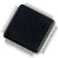
HD64F36077GHV Renesas Electronics America, HD64F36077GHV Datasheet - Page 71

HD64F36077GHV
Manufacturer Part Number
HD64F36077GHV
Description
16BIT MCU FLASH 56K, SMD, LQFP64
Manufacturer
Renesas Electronics America
Datasheet
1.HD64F36077GHV.pdf
(524 pages)
Specifications of HD64F36077GHV
No. Of I/o's
47
Ram Memory Size
4KB
Cpu Speed
20MHz
No. Of Timers
4
Digital Ic Case Style
LQFP
Supply Voltage Range
4.5V
Core Size
16bit
Program Memory Size
56KB
Oscillator Type
External Only
Controller Family/series
H8/300H
Peripherals
ADC
Rohs Compliant
Yes
Lead Free Status / RoHS Status
Lead free / RoHS Compliant
Available stocks
Company
Part Number
Manufacturer
Quantity
Price
Company:
Part Number:
HD64F36077GHV
Manufacturer:
RENESAS
Quantity:
340
Part Number:
HD64F36077GHV
Manufacturer:
RENESAS/瑞萨
Quantity:
20 000
- Current page: 71 of 524
- Download datasheet (4Mb)
(2)
Example 3: BCLR instruction executed designating port 5 control register PCR5
P57 and P56 are input pins, with a low-level signal input at P57 and a high-level signal input at
P56. P55 to P50 are output pins that output low-level signals. An example of setting the P50 pin as
an input pin by the BCLR instruction is shown below. It is assumed that a high-level signal will be
input to this input pin.
• Prior to executing BCLR instruction
• BCLR instruction executed
• After executing BCLR instruction
• Description on operation
1. When the BCLR instruction is executed, first the CPU reads PCR5. Since PCR5 is a write-only
2. Next, the CPU clears bit 0 in the read data to 0, changing the data to H'FE.
3. Finally, H'FE is written to PCR5 and BCLR instruction execution ends.
Input/output
Pin state
PCR5
PDR5
Input/output
Pin state
PCR5
PDR5
BCLR
register, the CPU reads a value of H'FF, even though the PCR5 value is actually H'3F.
As a result of this operation, bit 0 in PCR5 becomes 0, making P50 an input port. However,
bits 7 and 6 in PCR5 change to 1, so that P57 and P56 change from input pins to output pins.
To prevent this problem, store a copy of the PDR5 data in a work area in memory and
manipulate data of the bit in the work area, then write this data to PDR5.
Bit manipulation in a register containing a write-only bit
#0,
P57
Input
Low
level
0
1
P57
Output
Low
level
1
1
@PCR5
0
0
0
P56
Input
High
level
P56
Output
High
level
1
P55
Output
Low
level
1
0
P55
Low
level
1
0
Output
The BCLR instruction is executed for PCR5.
P54
Output
Low
level
1
0
P54
Output
Low
level
1
0
P53
Output
Low
level
1
0
P53
Output
Low
level
1
0
Rev. 1.00 Sep. 16, 2005 Page 41 of 490
P52
Output
Low
level
1
0
P52
Output
Low
level
1
0
P51
Output
Low
level
1
0
P51
Output
Low
level
1
0
REJ09B0216-0100
Section 2 CPU
P50
Output
Low
level
1
0
P50
Input
High
level
0
0
Related parts for HD64F36077GHV
Image
Part Number
Description
Manufacturer
Datasheet
Request
R

Part Number:
Description:
KIT STARTER FOR M16C/29
Manufacturer:
Renesas Electronics America
Datasheet:

Part Number:
Description:
KIT STARTER FOR R8C/2D
Manufacturer:
Renesas Electronics America
Datasheet:

Part Number:
Description:
R0K33062P STARTER KIT
Manufacturer:
Renesas Electronics America
Datasheet:

Part Number:
Description:
KIT STARTER FOR R8C/23 E8A
Manufacturer:
Renesas Electronics America
Datasheet:

Part Number:
Description:
KIT STARTER FOR R8C/25
Manufacturer:
Renesas Electronics America
Datasheet:

Part Number:
Description:
KIT STARTER H8S2456 SHARPE DSPLY
Manufacturer:
Renesas Electronics America
Datasheet:

Part Number:
Description:
KIT STARTER FOR R8C38C
Manufacturer:
Renesas Electronics America
Datasheet:

Part Number:
Description:
KIT STARTER FOR R8C35C
Manufacturer:
Renesas Electronics America
Datasheet:

Part Number:
Description:
KIT STARTER FOR R8CL3AC+LCD APPS
Manufacturer:
Renesas Electronics America
Datasheet:

Part Number:
Description:
KIT STARTER FOR RX610
Manufacturer:
Renesas Electronics America
Datasheet:

Part Number:
Description:
KIT STARTER FOR R32C/118
Manufacturer:
Renesas Electronics America
Datasheet:

Part Number:
Description:
KIT DEV RSK-R8C/26-29
Manufacturer:
Renesas Electronics America
Datasheet:

Part Number:
Description:
KIT STARTER FOR SH7124
Manufacturer:
Renesas Electronics America
Datasheet:

Part Number:
Description:
KIT STARTER FOR H8SX/1622
Manufacturer:
Renesas Electronics America
Datasheet:


