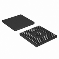
LH79524N0F100A1;55 NXP Semiconductors, LH79524N0F100A1;55 Datasheet - Page 28

LH79524N0F100A1;55
Manufacturer Part Number
LH79524N0F100A1;55
Description
IC, 32BIT MCU, 76.205MHZ, LFBGA-208
Manufacturer
NXP Semiconductors
Series
BlueStreak ; LH7r
Datasheet
1.LH79524N0F100A155.pdf
(64 pages)
Specifications of LH79524N0F100A1;55
Controller Family/series
(ARM7)
No. Of I/o's
108
Ram Memory Size
16KB
Cpu Speed
76.205MHz
No. Of Timers
3
No. Of Pwm Channels
3
Digital Ic Case Style
LFBGA
Core Size
32 Bit
Core Processor
ARM7
Speed
76.2MHz
Connectivity
EBI/EMI, Ethernet, I²C, IrDA, Microwire, SPI, SSI, SSP, UART/USART, USB
Peripherals
Brown-out Detect/Reset, DMA, I²S, LCD, POR, PWM, WDT
Number Of I /o
108
Program Memory Type
ROMless
Ram Size
16K x 8
Voltage - Supply (vcc/vdd)
1.7 V ~ 3.6 V
Data Converters
A/D 10x10b
Oscillator Type
External
Operating Temperature
-40°C ~ 85°C
Package / Case
208-LFBGA
Processor Series
LH795
Core
ARM7TDMI-S
Data Bus Width
32 bit
Mounting Style
SMD/SMT
3rd Party Development Tools
MDK-ARM, RL-ARM, ULINK2
Lead Free Status / RoHS Status
Lead free / RoHS Compliant
For Use With
SDK-LH79524-10-3216R - KIT DEVELOPMENT ZOOM SDK LH79524460-3474 - KIT DEV ZOOM STARTER FOR LH79524568-4305 - BOARD EVAL FOR LH79524
Eeprom Size
-
Program Memory Size
-
Lead Free Status / Rohs Status
Details
Other names
568-4332
935285053557
LH79524N0F100A1
935285053557
LH79524N0F100A1
LH79524/LH79525
Power Supply Sequencing
ommends that the 1.8 V power supply be energized
before the 3.3 V supply. If this is not possible, the 1.8 V
supply may not lag the 3.3 V supply by more than 100
µs. If longer delay time is needed, it is recommended
that the voltage difference between the two power sup-
plies be within 1.5 V during power supply ramp up. To
avoid a potential latchup condition, voltage should be
applied to input pins only after the device is powered-
on as described above.
DC SPECIFICATIONS
NOTES:
1. Table 2 details each pin’s buffer type.
2. Running Typical Application over operating range.
3. Current measured with CPU stopped and all peripherals enabled
Linear Regulator DC Characteristics.
28
VIH
VIL
VIT+
VIT-
VHYST
VOH
VOL
RIN
IACTIVE
ISTANDBY Standby current
ISLEEP
ISTOP1
ISTOP2
ISTOP2
ISTOP2
ISTOP2
IQUIESCENT Quiescent Current
ISLEEPLR
IOLR
VOLR
SYMBOL
When the linear regulator is not enabled, NXP rec-
SYMBOL
1
1
CMOS input HIGH voltage
CMOS input LOW voltage
Positive Input threshold voltage (Schmitt pins)
Negative Input threshold voltage (Schmitt pins)
Schmitt trigger hysteresis
Output drive (2 mA type)
Output drive (4 mA type)
Output drive (8 mA type)
Output drive (12 mA type)
Output drive (2 mA type)
Output drive (4 mA type)
Output drive (8 mA type)
Output drive (12 mA type)
Input leakage pull-up/pull-down resistors
Active current
Sleep current
Stop1 current
Stop2 current
Stop2 current
Stop2 current
Stop2 current
Current with Linear Regulator disabled
Output Current Range
Output Voltage, Linear Regulator
PARAMETER
PARAMETER
NXP Semiconductors
Rev. 01 — 16 July 2007
MIN. TYP. MAX. UNIT
0.0
MIN. TYP. MAX. UNIT
2.6
2.6
2.0
2.0
2.6
2.6
2.6
1.84
75
8
DC/AC Specifications
• -40°C to +85°C (Industrial temperature range)
• VDDC = 1.7 V to 1.9 V
• VDD = 3.0 V to 3.6 V, VDDA = 1.7 V to 1.9 V.
0.35
Unless noted, all data provided are based on:
420
115
3.8
40
85
50
95
45
25
200
5.5
0.8
0.4
0.4
0.4
0.8
mA
µA
µA
V
mA
mA
mA
kΩ
µA
µA
µA
µA
µA
V
V
V
V
V
V
V
V
V
V
V
V
V
CSEN = 1
IOH = -8 mA
IOH = -12 mA
IOH = 12 mA
CEN = 1
CEN = 1
CSEN = 1
CSEN = 1
IOH = -2 mA
IOH = -4 mA
IOL = 2 mA
IOL = 4 mA
IOL = 7 mA
VIN = VDD or GND (Calculate input
leakage current at desired VDD)
Note 2
Notes 2, 3
RTC ON, Linear Regulator ON
RTC OFF, Linear Regulator ON
RTC ON, Linear Regulator OFF
RTC OFF, Linear Regulator OFF
Preliminary data sheet
CONDITIONS
System-on-Chip


