LH79524N0F100A1;55 NXP Semiconductors, LH79524N0F100A1;55 Datasheet - Page 13
LH79524N0F100A1;55
Manufacturer Part Number
LH79524N0F100A1;55
Description
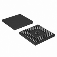
IC, 32BIT MCU, 76.205MHZ, LFBGA-208
Manufacturer
NXP Semiconductors
Series
BlueStreak ; LH7r
Datasheet
1.LH79524N0F100A155.pdf
(64 pages)
Specifications of LH79524N0F100A1;55
Controller Family/series
(ARM7)
No. Of I/o's
108
Ram Memory Size
16KB
Cpu Speed
76.205MHz
No. Of Timers
3
No. Of Pwm Channels
3
Digital Ic Case Style
LFBGA
Core Size
32 Bit
Core Processor
ARM7
Speed
76.2MHz
Connectivity
EBI/EMI, Ethernet, I²C, IrDA, Microwire, SPI, SSI, SSP, UART/USART, USB
Peripherals
Brown-out Detect/Reset, DMA, I²S, LCD, POR, PWM, WDT
Number Of I /o
108
Program Memory Type
ROMless
Ram Size
16K x 8
Voltage - Supply (vcc/vdd)
1.7 V ~ 3.6 V
Data Converters
A/D 10x10b
Oscillator Type
External
Operating Temperature
-40°C ~ 85°C
Package / Case
208-LFBGA
Processor Series
LH795
Core
ARM7TDMI-S
Data Bus Width
32 bit
Mounting Style
SMD/SMT
3rd Party Development Tools
MDK-ARM, RL-ARM, ULINK2
Lead Free Status / RoHS Status
Lead free / RoHS Compliant
For Use With
SDK-LH79524-10-3216R - KIT DEVELOPMENT ZOOM SDK LH79524460-3474 - KIT DEV ZOOM STARTER FOR LH79524568-4305 - BOARD EVAL FOR LH79524
Eeprom Size
-
Program Memory Size
-
Lead Free Status / Rohs Status
Details
Other names
568-4332
935285053557
LH79524N0F100A1
935285053557
LH79524N0F100A1


System-on-Chip
Preliminary data sheet
PIN NO.
117
116
119
118
115
114
113
112
104
103
102
100
110
109
106
111
130
131
80
79
78
77
76
74
73
72
71
70
69
67
65
63
62
61
99
98
97
96
95
94
93
91
11
14
17
A0
A1
A2
A3
A4
A5
A6
A7
A8
A9
A10
A11
A12
A13
A14
A15
D0
D1
D2
D3
D4
D5
D6
D7
SDCLK
SDCKE
DQM0
DQM1
nDCS0
nDCS1
nRAS
nCAS
nCS0/PM0
nCS1/PM1
nCS2/PM2
nCS3/PM3
nBLE0/PM4
nBLE1/PM5
nOE
nWE
USBDN
USBDP
AN0/UL/X+
AN1/UR/X–
AN2/LL/Y+/PJ3
SIGNAL NAME
TYPE
I/O
I/O
I/O
O
O
O
O
O
O
O
O
O
O
O
O
I
I
I
External Address Bus
External Data Bus
SDRAM Clock
SDRAM Clock Enable
Data Mask Output to SDRAMs
SDRAM Chip Select
SDRAM Chip Select
Row Address Strobe
Column Address Strobe
Static Memory Chip Select; multiplexed with GPO Port M[3:0]
Static Memory Byte Lane Enable / Byte Write Enable; multiplexed with
GPIO Port M[5:4]
Static Memory Output Enable
Static Memory Write Enable
USB Data Negative (Differential Pair output, single ended and Differential input)
USB Data Positive (Differential Pair output, single ended and Differential input)
ADC Input 0, 4 wire touch screen Upper Left, 5 wire touch screen X+
ADC Input 1, 4 wire touch screen Upper Right, 5 wire touch screen X–
ADC Input 2, 4 wire touch screen Lower Left, 5 wire touch screen Y+; multiplexed with
GPIO Port J3 (input only)
Table 5. LH79525 Pin Descriptions
NXP Semiconductors
Rev. 01 — 16 July 2007
DESCRIPTION
LH79524/LH79525
13
Related parts for LH79524N0F100A1;55
Image
Part Number
Description
Manufacturer
Datasheet
Request
R

Part Number:
Description:
NXP Semiconductors designed the LPC2420/2460 microcontroller around a 16-bit/32-bitARM7TDMI-S CPU core with real-time debug interfaces that include both JTAG andembedded trace
Manufacturer:
NXP Semiconductors
Datasheet:

Part Number:
Description:
NXP Semiconductors designed the LPC2458 microcontroller around a 16-bit/32-bitARM7TDMI-S CPU core with real-time debug interfaces that include both JTAG andembedded trace
Manufacturer:
NXP Semiconductors
Datasheet:
Part Number:
Description:
NXP Semiconductors designed the LPC2468 microcontroller around a 16-bit/32-bitARM7TDMI-S CPU core with real-time debug interfaces that include both JTAG andembedded trace
Manufacturer:
NXP Semiconductors
Datasheet:
Part Number:
Description:
NXP Semiconductors designed the LPC2470 microcontroller, powered by theARM7TDMI-S core, to be a highly integrated microcontroller for a wide range ofapplications that require advanced communications and high quality graphic displays
Manufacturer:
NXP Semiconductors
Datasheet:
Part Number:
Description:
NXP Semiconductors designed the LPC2478 microcontroller, powered by theARM7TDMI-S core, to be a highly integrated microcontroller for a wide range ofapplications that require advanced communications and high quality graphic displays
Manufacturer:
NXP Semiconductors
Datasheet:
Part Number:
Description:
The Philips Semiconductors XA (eXtended Architecture) family of 16-bit single-chip microcontrollers is powerful enough to easily handle the requirements of high performance embedded applications, yet inexpensive enough to compete in the market for hi
Manufacturer:
NXP Semiconductors
Datasheet:
Part Number:
Description:
The XA-S3 device is a member of Philips Semiconductors? XA(eXtended Architecture) family of high performance 16-bitsingle-chip microcontrollers
Manufacturer:
NXP Semiconductors
Datasheet:

Part Number:
Description:
The NXP BlueStreak LH75401/LH75411 family consists of two low-cost 16/32-bit System-on-Chip (SoC) devices
Manufacturer:
NXP Semiconductors
Datasheet:
Part Number:
Description:
The NXP LPC3130/3131 combine an 180 MHz ARM926EJ-S CPU core, high-speed USB2
Manufacturer:
NXP Semiconductors
Datasheet:
Part Number:
Description:
The NXP LPC3141 combine a 270 MHz ARM926EJ-S CPU core, High-speed USB 2
Manufacturer:
NXP Semiconductors
Part Number:
Description:
The NXP LPC3143 combine a 270 MHz ARM926EJ-S CPU core, High-speed USB 2
Manufacturer:
NXP Semiconductors

Part Number:
Description:
The NXP LPC3152 combines an 180 MHz ARM926EJ-S CPU core, High-speed USB 2
Manufacturer:
NXP Semiconductors
Part Number:
Description:
The NXP LPC3154 combines an 180 MHz ARM926EJ-S CPU core, High-speed USB 2
Manufacturer:
NXP Semiconductors

Part Number:
Description:
Standard level N-channel enhancement mode Field-Effect Transistor (FET) in a plastic package using NXP High-Performance Automotive (HPA) TrenchMOS technology
Manufacturer:
NXP Semiconductors
Datasheet: